Huawei has changed the standard for semiconductors.
There is an open secret in the semiconductor industry: Moore's Law is approaching its limit.
This fact is tacitly acknowledged by the industry. Over the past 60 years, the underlying law that the entire industrial chain, from Intel, TSMC to ASML, has relied on is facing challenges.
Today, the gate width of the most advanced nanoscale chips is only about a dozen silicon atoms. If it gets any smaller, due to the existence of the quantum tunneling effect, electrons will no longer be effectively confined by the semiconductor.
The path of continuously shrinking the process has been taken for sixty years. Everyone knows where the end is, but no one is willing to publicly admit it.
Until May 25, 2026, He Tingbo, a director of Huawei and the president of the Semiconductor Business Unit, announced a new semiconductor evolution principle:
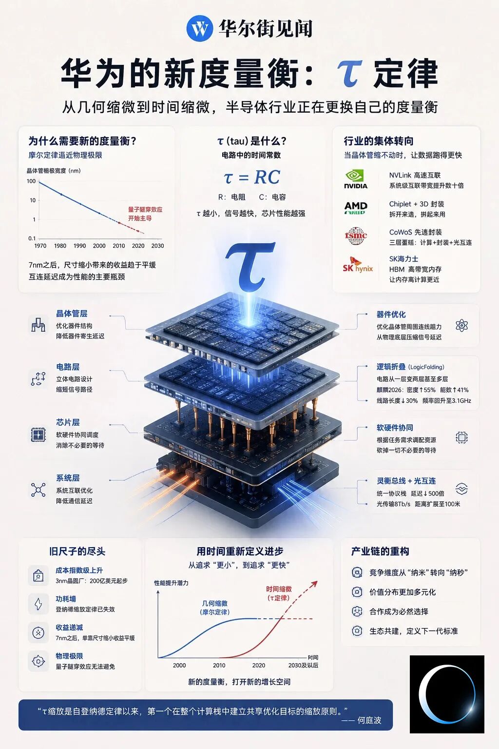
Tao (τ) Law. Its core proposition is to replace the "geometric scaling" of Moore's Law with "time scaling".
As Moore's Law approaches its limit, He Tingbo believes that a new path is worth exploring. That is, instead of pursuing the shrinkage of transistors, make the signals travel faster.
Based on this path, Huawei has mass - produced 381 chips in the past six years. The new - generation Kirin chips to be released this autumn will achieve a more than 50% jump in transistor density without changing the process. By 2031, Huawei plans to make the transistor density of its chips reach the same level as that of the 1.4 - nanometer process, using this very methodology.
In fact, Tao Law did not appear out of thin air. From NVIDIA to TSMC, from AMD to SK Hynix, the entire semiconductor industry has been groping in the same direction for nearly a decade.
Huawei's statement this time officially outlines a clear framework and standard for this exploration for the first time.
I
The End of the Old Path
τ (tau) is called the "time constant" in circuit theory.
There are billions of transistors in a chip, and they are connected by metal wires. Signals travel along the wires, but the wires have resistance. The longer the wire, the greater the resistance, and the slower the signal.
Therefore, the smaller the τ, the faster the signal and the stronger the chip performance.
In the process of transistor shrinkage over the past few decades, in essence, it not only increased the transistor density but also synchronously reduced the parasitic capacitance and signal propagation delay. Therefore, the RC time constant has been in a downward trend for a long time.
The idea of Tao Law is full of the flavor of the first - principles thinking. Since the goal is to reduce τ to improve efficiency, besides making the transistors smaller, it is obviously also possible to achieve compression in other dimensions.
He Tingbo disassembled τ into four layers: the transistor layer, the circuit layer, the chip layer, and the system layer. There are different ways to compress time at each layer.
The reason why Tao Law firmly takes this new path is that the old path has reached its end.
In 1965, Gordon Moore predicted that the number of transistors in an integrated circuit would approximately double every two years. Moore's Law is not only an industrial law but also an industrial consensus. Everyone developed, invested, and built factories according to this rhythm, and finally made the prediction self - fulfilling.
It also had a perfect partner in the early days: Dennard Scaling Law, which states that after the transistors shrink, the power density remains unchanged. This means that not only is the chip faster, but the heat generation is also controllable.
The combination of these two laws formed the underlying belief of the information industry for half a century.
Throughout the entire industrial chain from design, manufacturing to equipment and materials, everyone is running on the same track. The advanced nanoscale process has gradually become the power coordinate of the entire industry. Companies that can produce chips with the most advanced processes are more likely to stand at the top of the food chain.
Dennard Scaling collapsed around 2005. People found that it was difficult to control the heat generation of chips when the size was too small. This ultimately made Intel abandon the frequency - based thinking and start to turn to the multi - core route.
The rise of the smartphone era did make Moore's Law hold up for a longer time.
However, after entering the single - digit nanometer era, each step of scaling down means an exponential increase in cost and difficulty. The construction cost of a 3 - nanometer wafer factory starts at tens of billions of dollars, and there are now only a handful of players in the world who can afford it.
He Tingbo wrote more straightforwardly in the paper:
After 7 nanometers, the benefits brought by pure size reduction have leveled off.
As the advanced process enters the deep - water zone, the proportion of interconnection delay, power consumption, and data transfer cost in the system performance is getting higher and higher. Moreover, the cost increase problem caused by relying solely on the advanced process is becoming more and more difficult to control.
As a result, the core promise that has supported the industry for the past half - century, "producing more transistors at a lower cost with each generation", is no longer achievable.
II
How Participants Break Through
Heavyweight players in the industry have all launched breakthrough attempts in this direction.
The earliest and most radical one is NVIDIA's commitment to cluster expansion.
In 2016, NVIDIA introduced a high - speed inter - GPU interconnect bus called NVLink on the P100 of the Pascal architecture. Jensen Huang aimed to solve the pain point of data transmission between GPUs.
Looking back ten years later, this bet was accurate. From the first - generation NVLink to the fifth - generation of the Blackwell architecture in 2024, the inter - GPU interconnect bandwidth has increased by dozens of times.
The GB200 NVL72 connects 72 GPUs into a whole using the fifth - generation NVLink. The two - way interconnect bandwidth of a single GPU is 1.8TB/s, and the total bandwidth of the entire NVLink domain exceeds 130TB/s. NVIDIA even uses NVLink - C2C to directly solder the GPU and CPU together, sharing a unified memory space.
At the first press conference, Jensen Huang was also more willing to spend time talking about "interconnection" rather than just "computing power".
AMD took another path.
In 2019, the Zen 2 architecture began to split the processor into multiple small chips for separate manufacturing and then package them together, aiming to break through the photomask size limit and ensure a stable yield. This concept named Chiplet has gone further in AI chips: The MI300X released at the end of 2023 uses TSMC's 3D packaging technology to vertically stack multiple computing dies and I/O dies together. A single package integrates 153 billion transistors and 192GB of HBM3 memory.
AMD no longer focuses solely on the advanced process. Instead, it uses the method of "manufacturing separately and using together" to achieve an integration level that a single chip could not achieve in the past at the packaging level.
TSMC's shift is also obvious.
For many years, TSMC's advanced - process narrative has been about continuous shrinkage, from 5nm to 3nm, and then to 2nm.
However, since 2023, the proportion of advanced packaging in TSMC's capital expenditure and strategic narrative has increased rapidly.
The CoWoS packaging technology, which aims at bandwidth density and attaches GPU chips and HBM memory closely together, has long been in short supply in production capacity and has become an important part of AI chip shipments.
At the 2026 technology forum, TSMC announced a three - layer "cake" AI platform architecture: the bottom layer for computing, the middle layer for packaging integration, and the top layer for photonic interconnection. The COUPE technology on the top layer uses optical signals to replace electrical signals for transmission between chips, improving energy efficiency by several times and reducing latency by an order of magnitude. The king of the process has started to tell stories about packaging and optics.
The arms race among memory manufacturers is even more intense.
The competition between SK Hynix and Samsung around HBM has a core goal of making the memory closer to the computing unit and feeding data faster. From HBM2 to HBM3 and then to HBM3E, each generation has been stacking memory chips higher and attaching them closer to the GPU.
The next - generation HBM4 will introduce hybrid bonding technology, eliminating the need for solder bumps. Copper will be directly connected at the atomic level, increasing the interconnection density by one to two orders of magnitude.
In addition, there are Intel's Foveros 3D packaging, the industry - jointly promoted UCIe die - to - die interconnect standard, and the accelerated industrialization of silicon - photonics interconnection.
The entire industry is actually adjusting its direction and challenging a common goal:
When the transistors can no longer be shrunk, make the data travel faster.
In the past decade, the focus of research and development has begun to shift from "manufacturing smaller switches" to "building faster roads".
III
Huawei's Strengths and Positioning
In this industry - level breakthrough, Huawei is in a very special position.
The restriction on advanced lithography equipment has made Huawei face a problem earlier and more urgently than others. If process scaling becomes an obstacle, how can the target efficiency be achieved through engineering design?
However, this is actually an advantage for Huawei, which has a background in communications.
One of the core capabilities that Huawei has accumulated over the decades, from program - controlled switches to 5G base stations, is to organize a large number of scattered nodes into a coordinated system.
As the data centers in the AI era are becoming more and more like a super - large communication network, Huawei's strengths suddenly have new strategic value.
In the four - layer optimization system, the entry point at the device layer is also to optimize the resistance of the wiring around the transistors and compress the signal delay from the physical bottom layer.
At the circuit layer, Huawei uses a method called Logic Folding.
In traditional chip circuits, the signals run left and right on a flat plane. The longer the wiring, the slower the signal. Logic Folding unfolds the circuit from one layer to two layers, like folding a piece of paper in half. The signal path that originally had to run a long way horizontally becomes a direct vertical path after folding.
According to the measured data of Kirin 2026, the transistor density has increased by more than 50% in a single generation, the energy efficiency has increased by 41%, the CPU frequency has returned to 3.1GHz, the cache frequency has increased by more than 40%, and the length of the core circuit has been shortened by about 30%. There are plans for three - layer and four - layer folding in the future, and the frequency is expected to break through 4GHz by 2029.
This is similar to AMD's 3D die stacking and Intel's Foveros methodology in that they all move from a two - dimensional to a three - dimensional structure. The difference is that AMD and Intel stack multiple different chips vertically, while Huawei folds the circuit inside the same chip.
At the chip layer, Huawei coordinates software, architecture, and chips.
That is, it allocates the internal resources of the chip according to the actual task requirements and eliminates all unnecessary waiting. Just like NVIDIA's in - depth collaboration in the CUDA ecosystem and AMD's progress in ROCm, they are all different solutions to the same problem.
The system layer may be where Huawei's unique genes play the greatest role.
The Lingqu Bus was launched after six years of development since its project initiation in 2019. It uses a unified protocol to replace the overlapping communication protocol stacks in the AI cluster. The measured result is that the system communication delay has been reduced from dozens of microseconds to about 100 nanoseconds, a reduction of nearly 500 times.
On top of the Lingqu Bus, the Hi - ONE optical interconnection engine uses optical signals instead of copper wires to transmit data. The bandwidth of a single module is 8Tb/s, and the transmission distance has been extended from less than 1 meter to 100 meters.
Comparing with NVIDIA: NVIDIA uses a hierarchical combination of NVLink + NVSwitch + InfiniBand to solve the interconnection problem, while Huawei's Lingqu Bus uses a single protocol to connect all levels.
NVIDIA's GB200 NVL72 connects 72 GPUs into a whole, while Huawei's Atlas 960 SuperPod uses the Lingqu Bus to connect 15,488 Ascend cards into a super - node.
Both companies, starting from their own technologies, are actually heading towards the same destination: to make tens of thousands of cards work together like a single machine.
He Tingbo's personal experience is also a microcosm of Huawei's chip destiny. She joined Huawei in 1996 to work on optical communication chips. In 1998, she went to Shanghai alone to form a 3G chip team and then worked in Silicon Valley for two years. Since then, she has long been in charge of HiSilicon.
When facing the supply - chain crisis in 2019, it was He Tingbo who sent that famous internal letter about "turning the spare tire into the main tire". She is not only the soul figure of Huawei's chip business but also the person who has deeply felt the pain of process restrictions.
In a sense, Tao Law is also a product of this pressure.
IV
System and Chain Reconstruction
What Tao Law does is actually to define the collective shift of the industry in a more systematic way over the years.
NVIDIA has invested ten years in NVLink to solve the τ at the system layer. TSMC's CoWoS and 3D packaging address the τ at the circuit and chip layers. SK Hynix's HBM aims to solve the τ between storage and computing. AMD's Chiplet is to solve the τ of communication between chips.
Each company is compressing time from its own perspective, but no one has previously integrated and narrated these efforts at a system - level in the same coordinate system.
The special thing about Huawei's Tao Law is that it has established this coordinate system. He Tingbo wrote a weighty sentence in the paper:
τ scaling is the first scaling principle since Dennard's Law to establish a shared optimization goal across the entire computing stack.
As the function of Moore's Law as a unified coordinate system gradually weakens, the entire industry really needs a new ruler.
Over the past sixty years, the semiconductor industry has mainly used the nanoscale process as a ruler to measure progress. This ruler is simple and powerful, but it has actually been measuring a non - fundamental proxy indicator. Transistor shrinkage itself is not the goal. Higher computing power density and shorter signal propagation time are.
However, this ruler can no longer be scaled down now.
Changing the ruler means a redistribution of power. In the past, the companies at the top of the food chain were those that mastered the most advanced processes. In the dimension of "time scaling", packaging factories, memory factories, interconnect protocol definers, and system architects may all participate in the game that was once only for the cutting - edge processes.
TSMC's advanced process still has irreplaceable value, but Tao Law has changed it from the only option to one of many choices.
He Tingbo finally said: "The future definitely belongs to open cooperation. On the path of semiconductor evolution, no single enterprise can find all the answers alone."
Just as the CUDA ecosystem is co - created by users, the construction of Tao Law also requires an ecosystem.
Just as NVIDIA needs TSMC's packaging, TSMC needs SK Hynix's HBM, SK Hynix needs the yield improvement of hybrid bonding equipment manufacturers, and Huawei's Lingqu Bus also depends on the enrichment of the supply chain such as optical modules.
The four - layer optimization system depicted by Tao Law belongs to different industrial links at each layer, and this will drive another reconstruction of the semiconductor industrial chain.
Over the