If the industry doesn't follow Huawei's Tao's Law, how can it reach 0.2nm?
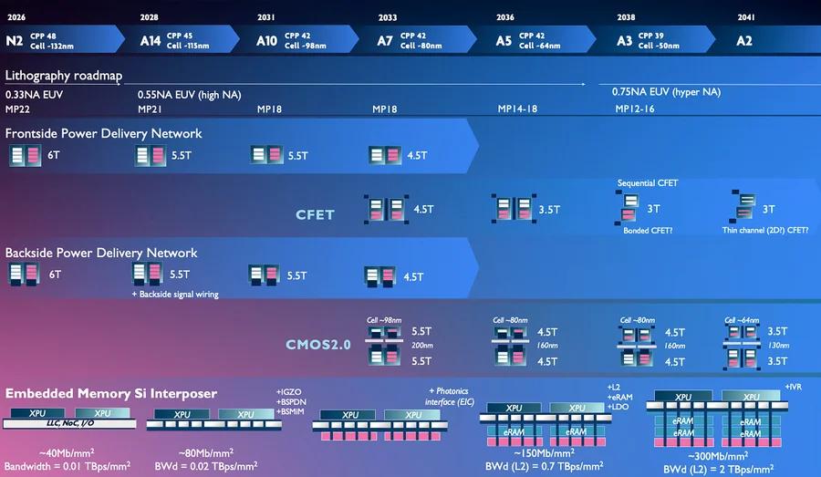
Today, Huawei released the "Tao (τ) Law", which uses time micro - reduction to replace geometric micro - reduction, and plans to achieve the same transistor density as the 1.4nm process in 2031. Two days ago, the Interuniversity Microelectronics Centre (imec) released a 15 - year technology roadmap, covering seven process nodes from N2 (2 nanometers) to A2 (2 angstroms, i.e., 0.2 nanometers), outlining the technological evolution direction of the semiconductor industry in the next 15 years.
If Huawei's Tao Law represents a brand - new technological path, then imec's roadmap shows a more mature traditional evolution path. To understand this roadmap, one cannot just look at the node names and years. What really deserves in - depth exploration is what the three major wafer fabs are doing behind each technological turning point, the differences in their routes, and how these technological evolutions will reshape the entire industrial landscape.
01 2026 - 2033: Three Key Points
Lithography Machine: To Buy or Not to Buy, and When?
The lithography machine is the heart of chip manufacturing. In this long - march towards 0.2 nanometers, ASML plays a key role. The current mainstream EUV lithography machines (NXE series) use a numerical aperture (NA) of 0.33, which has supported the production from 7nm to 3nm. However, as the process continues to shrink, the resolution of 0.33NA EUV becomes insufficient. When the metal pitch shrinks below 30nm, it can only be achieved through complex processes such as double exposure, which significantly increases the cost and yield risk.
High NA EUV (0.55NA) is the next threshold that must be crossed. From 0.33 to 0.55, the NA value increases by about 66%, and the resolution can be improved from 13nm to 8nm. More importantly, a larger NA value means higher light collection efficiency, and a single exposure can complete the patterning that previously required multiple exposures. The efficiency improvement is revolutionary. Data disclosed by ASML shows that High NA EUV only needs one exposure and a single - digit number of processing steps to complete the work that early machines required three exposures and about 40 processing steps for.
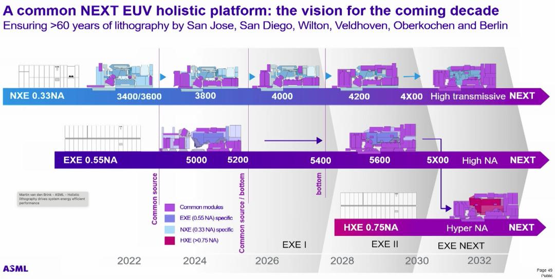
After this path, Hyper NA EUV (0.75NA) is the next milestone. The roadmap shows that 0.75NA EUV is expected to be introduced after 2038, corresponding to a metal pitch of 12 - 16 nanometers. At that time, 0.55NA and 0.75NA will form a combination, covering the main process windows from A14 to A3.
Before the large - scale popularization of High NA EUV, different manufacturers show obvious differences in their procurement rhythms. Intel is the most aggressive bettor. In February 2025, Intel announced that its first two Twinscan EXE:5000 had been put into production in the factory, producing 30,000 wafers within a quarter, and the reliability was nearly doubled compared to the previous generation. Intel plans to use it for the first time in the 18A process and fully introduce it in the 14A process. TSMC said "it's too expensive, so we won't buy it". TSMC clearly stated that all process nodes from N2 to A13 (1.3 nanometers) do not require High NA EUV, and the existing EUV equipment can be used until at least 2029. TSMC's reason is very practical: the unit price of High NA EUV is as high as about $400 million, twice that of the existing EUV. Currently, TSMC has more than 100 EUV lithography machines, and replacing all of them would require an investment of tens of billions of dollars. TSMC chooses to use the mature EUV multiple - exposure technology for the transition and waits for a more cost - effective time for the equipment. Samsung originally planned to start mass - producing the 1.4 - nanometer process (SF1.4) in 2027, but now it has adjusted the target to 2029. Previously, Samsung had installed the first EXE:5000 in its Hwaseong factory in South Korea, mainly for technology R & D.
From the perspective of the entire industry, the large - scale popularization of High NA EUV is expected to be around 2027 - 2028, when the cost and capacity issues will gradually be alleviated. But before that, the game around "to buy or not to buy, and when to buy" will directly affect each company's technology roadmap and cost structure.
Back - side Power Delivery Network: Three Timetables for Three Major Manufacturers
Inside the chip, wiring is an art. Signal lines are needed to transmit data between transistors, power lines are needed to supply power, and ground lines are needed to complete the circuit. In the traditional design, all these lines are on the front side of the wafer, just like a city where the ground is full of various vehicles.
When this path reaches the N2 and lower nodes, problems start to emerge. The idea of back - side power delivery is very simple: move the power network to the back side of the wafer, and only signal lines are on the front side.
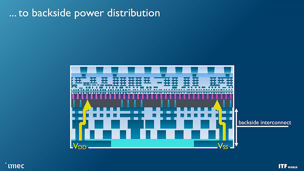
The roadmap shows that the basic back - side power delivery technology will be introduced from A14, the complete separation of signal wiring and power delivery will be achieved at the A10 node, and the via density and power delivery efficiency will continue to be optimized at the A7 and more advanced nodes. Meanwhile, imec is also researching how to further improve the heat dissipation performance of back - side power delivery.
Of course, this technology also brings new challenges: wafer deformation in the back - side process may affect the alignment accuracy with the front side; the etching and filling of TSVs with high aspect ratios require brand - new process capabilities; and the thermal management scheme also needs to be redesigned. But all these challenges have clear solutions, and the industry is expected to gradually overcome them between 2026 and 2030.
The mass - production timetables of different companies are slightly different: Intel is the most aggressive, applying the PowerVia technology for the first time in the 18A process in 2025. According to Intel's disclosure at the VLSI Symposium, PowerVia directly delivers power to the back side of the transistor through back - side vias. Tests show that it can reduce the voltage drop (IR drop) by more than 30% and at the same time free up the front - side wiring space. TSMC's plan is set for the second half of 2026, introducing the Super Power Rail (SPR) back - side power rail technology at the A16 node. A16 is a 1.6 - nanometer - level process, regarded as a transitional node between 2nm and 1.4nm. TSMC claims that after adopting back - side power delivery, in a 2nm mobile processor design, compared with front - side power delivery, the voltage drop is reduced by 122 millivolts, resulting in a 22% area saving, while improving performance and energy efficiency. Samsung has chosen a more conservative strategy, and the SF2Z back - side power delivery node will be mass - produced in 2027. According to Samsung's disclosure at the foundry forum, SF2Z not only improves the PPA comprehensive parameters but also significantly reduces the circuit voltage drop, and is specially designed for HPC and AI chips. Samsung's 2nm process family timetable is as follows: the SF2 mobile version will be launched in 2025, the SF2P improved version in 2026, and the SF2Z with back - side power delivery in 2027.
Storage Upgrade: The Technical Route Disagreement Behind a 200 - fold Increase in Bandwidth
The evolution of embedded storage may be the most easily overlooked but most influential part of the entire roadmap on chip performance. According to the roadmap, the storage density will increase from 40 Mb/mm² in 2026 to 300 Mb/mm² in 2041 (7.5 times), and the bandwidth will jump from 0.01 TBps/mm² to 2 TBps/mm² (200 times). Behind this figure is the complete redesign of the entire storage architecture.
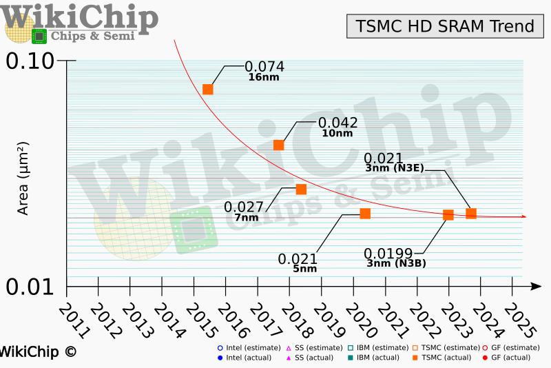
In the past few years, the miniaturization of SRAM has encountered serious bottlenecks. The HD SRAM bit - cell size of TSMC's N3B process is 0.0199µm², only about 5% smaller than the 0.021µm² of N5; the N3E has even regressed to 0.021µm², basically the same as N5. This means that at the 3nm node, SRAM has almost stopped shrinking.
The root cause of the problem is that SRAM cells need to maintain stability and high yield. When the transistor size shrinks to a certain extent, process variability begins to dominate, leading to an increase in the read - write error rate. The industry once pessimistically believed that SRAM miniaturization had reached its end.
The turning point came at the N2 node. TSMC announced that the HD SRAM bit - cell size of its N2 process has shrunk to 0.0175µm², achieving a density of 38 Mb/mm², a significant improvement compared to N3/N5. The key driving force is the introduction of GAA nanosheet transistors. The all - around gate structure improves electrostatic control, helps reduce leakage, and thus maintains the reliability of SRAM at a smaller size. In contrast, the SRAM density of Intel's 18A process is about 31.8 Mb/mm² (0.021µm² bit - cell), closer to TSMC's N3 than N2. This gap may affect Intel's competitiveness in the high - performance processor market, as modern CPUs and GPUs are increasingly dependent on caches.
When SRAM miniaturization encounters bottlenecks, new embedded storage technologies are accelerating towards mass production.
eMRAM (embedded magnetoresistive random - access memory) is the most mature choice at present. GlobalFoundries has achieved mass production of eMRAM on the 22nm FDSOI platform, mainly for automotive and IoT applications. Compared with eFlash, eMRAM has a 1000 - fold increase in write speed, a 400 - fold reduction in power consumption, and does not require an additional erase cycle. TSMC is also actively deploying. The 32Mb MRAM uses the 22nm ULL logic platform, with a read - write speed of 10ns and can withstand 1 million cycles of write operations.
ePCM (embedded phase - change memory) is the main focus of STMicroelectronics. In 2024, ST announced that the 18nm FD - SOI ePCM MCU started to provide samples to customers to break through the 20nm process barrier of MCUs. The advantage of ePCM is that its structure is hardly affected by the underlying CMOS and can be more flexibly integrated with advanced logic processes.
eRRAM (embedded resistive random - access memory) is the focus of the cooperation between Infineon and TSMC. The two parties are developing 28nm eRRAM, mainly targeting the automotive MCU market.
These three technical routes have their own trade - offs: eMRAM has the fastest speed and the best durability, but the manufacturing cost is relatively high; ePCM has the highest density, but the write power consumption is relatively high; eRRAM has the best compatibility with the standard CMOS process, but there is still room for improvement in durability and retention. The future of embedded storage will not be a one - size - fits - all situation, and different application scenarios will give rise to different technology combinations.
02 2033 (A7 Node): Continuous Evolution of Chip Architecture
CFET: The Ultimate Form of Transistor Architecture
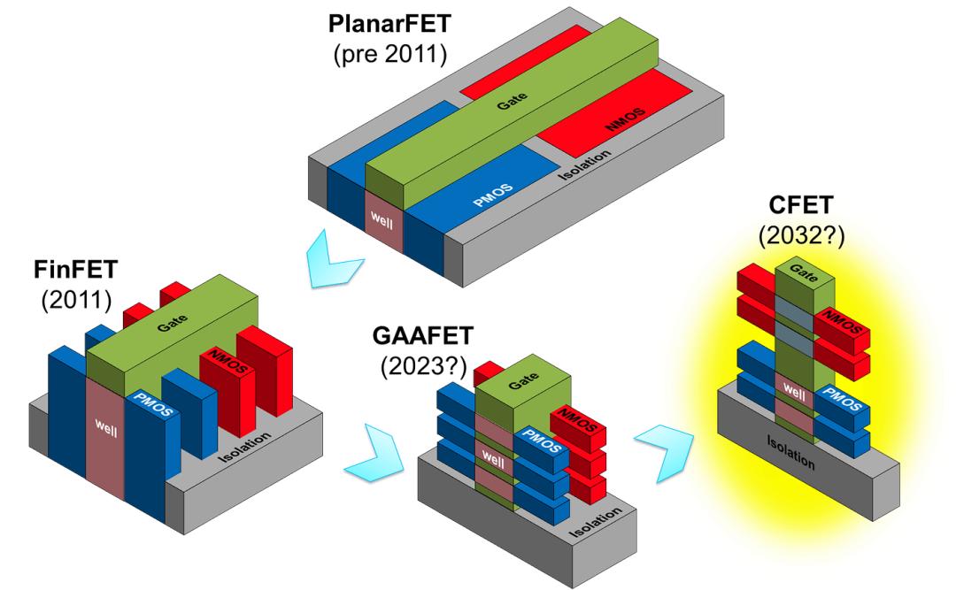
Starting from 2033, the roadmap enters the real deep - water area - CFET (Complementary FET) officially makes its debut. To understand CFET, one needs to first understand its predecessors.
FinFET has dominated the chip industry since 2011. Intel was the first to achieve the mass - production commercialization of 22nm FinFET in 2011. The tri - gate structure improved the electrostatic control of the channel and supported the entire era from 22nm to 3nm. However, when the fin width shrinks to a few atomic diameters, the problems of leakage current and variability reappear.
GAA nanosheets are the natural successors of FinFET. Starting from the N2 node in 2025, TSMC, Samsung, and Intel will all adopt the all - around gate nanosheet structure. The transistor channel is no longer a "fin" but a thin sheet completely wrapped by the gate, with better electrostatic control and low leakage at a smaller size. TSMC's N2, Samsung's SF2, and Intel's 18A are all based on GAA nanosheets.
CFET takes it a step further: it stacks n - type (NMOS) and p - type (PMOS) transistors vertically, sharing the source - drain region. This means that nearly twice as many transistors can be placed in the same silicon area.
imec's demonstration shows that the transistor density of the CMOS logic circuit with the CFET architecture is expected to be 1.6 to 1.8 times that of the nanosheet FET. The significance of this figure is that it is not a minor improvement on the existing architecture but a real revolution in area density.
The CFET competition among the three major manufacturers has started in advance. Intel has demonstrated a unique solution of stacking NMOS on PMOS, combined with back - side power delivery and back - side contact, to maximize area and power efficiency. The yield of its vertically stacked NMOS/PMOS nanosheet transistors exceeds 90%, achieving high on - state current and low leakage, with a switching current ratio of more than six orders of magnitude.
TSMC has announced that its 48nm CPP (contact poly pitch) has met the standard, which is a key threshold for CFET commercialization. By introducing vertical isolation between NMOS/PMOS and appropriate internal spacers between the gate and the source/drain, TSMC's vertically stacked structure has a yield of more than 90%, showing healthy device characteristics.
Samsung's CFET roadmap is relatively low - key, but considering its aggressive history in GAA technology (Samsung was the first to introduce the GAA architecture in the 3nm process), it is possible that it has made early arrangements.
The manufacturing challenges of CFET should not be underestimated. The high - aspect - ratio structure brings a