The PCB has been rising continuously. What changes have taken place in the narrative logic?
Recently, the market performance has been dominated by silicon-based products, and there has been little else. The entire market is shrouded in a sense of anxiety and fear under the dominance of silicon-based products.
A prominent feature of this K-shaped differentiated market is that older investors can no longer bear it. Stocks favored by them are continuously being sold off in a slow decline, and they are chasing the silicon-based industries represented by semiconductors.
There's no need to overthink whether this is a characteristic of the market's peak. As we've said before, the market is severely punishing investors who don't bet on AI. It's not embarrassing to join now. All you need to do is to keep track of the industry.
The silicon-based sector has been booming in multiple areas recently. There's no need to elaborate on semiconductor equipment and foundry. Recently, another sector has shown a sharp upward trend, namely the PCB sector. This sector has always been strong because PCB is the cornerstone of interconnection for electronic devices and is also a core hardware component for AI.
Last Friday, the PCB sector saw a collective daily limit, and its performance remains very strong today. What new changes in the narrative logic have led to this sharp upward trend again?
01 The Explosive Increase in PCB Value Brought by NVIDIA's VR200
This round of price increase is due to Morgan Stanley's analysis of NVIDIA's supply chain. In the material structure of its next-generation AI platform, the VR200 NVL72 cabinet (which is currently in the production ramp-up phase), the value of PCB has increased by 233%, second only to that of storage. Naturally, the market has gone into a frenzy.
Because this is not just a grand and visionary concept but more importantly, it represents a visible increase in value in the future.
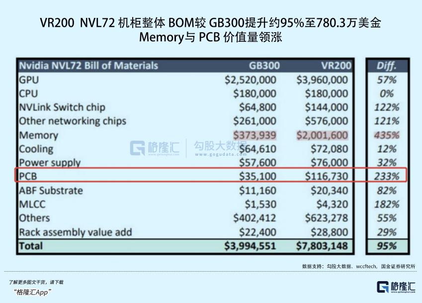
According to Morgan Stanley's research and analysis, the value of PCB per VR200 cabinet has soared from approximately $35,100 for the GB300 to about $116,700. This increase is not only a simple increase in quantity but also an expansion of product categories. The increase comes from the upgrade of the computing board layer from 22L HDI to 26L, the upgrade of the CCL material grade from M7 to M8, and the increase of the PCB for the switch tray from 24L to 32L. At the same time, a 44-layer Midplane PCB and supporting boards for ConnectX and BlueField modules have been newly added, and both the process complexity and the single-board area have increased significantly.
From the perspective of single-board value, the core scale of PCB in the VR200 era has achieved an all-round leap compared to that of the GB300. The copper-clad laminate material has been upgraded from M8 to M9, and with the upgrade of the copper foil system from HVLP3 to HVLP4/5 and the introduction of stone cloth and special resins, the central cost of materials has increased significantly. The number of layers has jumped from the common 20 - 30 layers in the GB300 era to 44 layers or even more than 78 layers in the VR200 era. Doubling the number of layers has directly led to a twofold leap in process difficulty and single-board value. Meanwhile, the increase in board thickness and material hardness has significantly increased the demand for over-sized mechanical drill bits and ultra-fast laser drilling equipment in the drilling process. The proportion of drill bit consumable costs has increased, which is 5 - 8 times the traditional consumption.
The explosive increase in PCB value represented by VR200 is just the first step in the generational upgrade of NVIDIA's AI hardware.
The next-generation Rubin Ultra platform will adopt a brand-new Kyber cabinet architecture and is expected to enter mass production in the second half of 2027.
It will be comprehensively upgraded in terms of architecture, power supply, packaging, etc., driving the continuous growth of PCB value on a high base. The power consumption of the entire Kyber cabinet reaches 600kW, and its computing power is 14 times that of the GB300, posing higher requirements for PCB.
The innovation of the power supply architecture has generated new demands. The Kyber uses 800VDC high-voltage direct current power supply to replace the traditional 54VDC architecture, improving energy efficiency by 5% and reducing maintenance costs by 70%. At the same time, it has spawned a new category of PCB for high-voltage and high-current power supply, further enriching the product matrix. In terms of materials, M9-grade copper-clad laminates and quartz cloth are fully penetrated, and the value of the single board of the Compute Blade continues to increase. The 78-layer M9-grade orthogonal backplane replaces copper cables, and PCB has become the core interconnection carrier at the rack level for the first time, achieving a breakthrough in specifications by an order of magnitude.
The CoWoP packaging technology has redefined the functional positioning of PCB. The Chip-on-Wafer-on-PCB (CoWoP) technology breaks the boundary between PCB and packaging substrates, allowing PCB to directly undertake the chip-level packaging function, shortening the signal path and improving thermal management and power integrity. This change has upgraded PCB from a system interconnection component to a chip packaging carrier, bringing its value positioning closer to that of the semiconductor level and further raising the industry barrier.
The coupling of M9 materials, mSAP process, and CoWoP technology has become the core engine for the development of AI PCB. The Panasonic MEGTRON 9 copper-clad laminate is suitable for a single-channel rate of 224Gbps, supporting the mass production of ultra-high multi-layer backplanes. The mSAP process ensures the processing of fine circuits. The CoWoP promotes functional upgrades. PCB simultaneously undertakes the three functions of signal, power supply, and packaging, and the value per cabinet continues to multiply. The competition logic in the industry has shifted from scale to technical barriers.
It can be said that as the core carrier for high-speed signal interconnection, thermal management, and structural integration, the technical barriers and value elasticity of PCB will be significantly magnified in the new generation of AI products. Manufacturers of high-layer HDI and high-order CCL in the industrial chain are expected to obtain excess returns.
02 The Continuous Optimization of the PCB Industry Structure, with Domestic Manufacturers Benefiting from Industry Increment and Domestic Substitution
The development of AI has not only improved the quantity and quality of the industry but also promoted the continuous optimization of the industry structure, showing three major trends: concentration at the top, domestic substitution, and industrial chain collaboration. Globally, manufacturers with the mass production capacity of semiconductor-grade PCB are highly concentrated. Leading enterprises seize the market with their technological, production capacity, and customer advantages, while domestic manufacturers are constantly capturing a larger market share with continuous technological upgrades and cost advantages.
High-end AI PCB has high technical barriers and a long certification cycle. Only a few global enterprises have the mass production capacity, and the market share is concentrated at the top. Manufacturers such as Shengyi Technology, Dongshan Precision, and others have deeply bound with global AI giants with core technologies such as mSAP, high-layer backplanes, and CoWoP adaptation, and are the first to enjoy the industry dividends. Small and medium-sized manufacturers find it difficult to enter the high-end market, resulting in a K-shaped differentiation in the industry. The clearance of low-end production capacity is accelerating, which is conducive to the concentration of market share at the top and the optimization of the industry structure.
The process of domestic substitution is also accelerating. China is the world's largest PCB production base and has gradually broken through technical bottlenecks in the high-end field. Shenghong Technology, Jingwang Electronics, and Guanghe Technology have achieved mass production of high-multi-layer server boards and entered the global supply chain. Shengyi Technology and Nanya New Materials have broken through the M9-grade CCL technology, breaking the overseas material monopoly. Drill bit enterprises such as Zhongwu Gaoxin and Dingtai Gaoke have benefited from the explosive demand for consumables. The coordinated upgrade of the entire chain has promoted the transformation of the domestic industry from scale leadership to technology leadership.
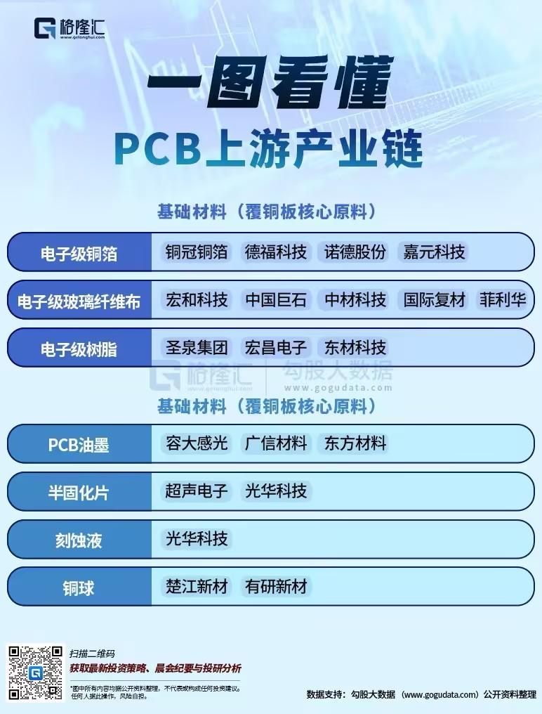
The upstream and downstream of the industrial chain are growing in a coordinated manner. The explosive growth of PCB value has led to a surge in the demand for upstream copper-clad laminates, copper foils, electronic cloth, drill bits, etc., and the supply and demand of high-end materials are in short supply. The gross profit margin of high-end products of midstream manufacturing enterprises has increased. Downstream AI servers have achieved performance optimization through PCB upgrades. The entire chain has formed a demand resonance, jointly promoting the high-quality development of the industry.
Today, the International Symposium on Circuits and Systems was held in Shanghai. He Tingbo, the chairman of Huawei and the president of the Semiconductor Business Department, officially announced the "Tao's Law" in a keynote speech titled "Exploration and Practice of New Paths in Semiconductors." This is the first time that China has proposed a new principle to guide the development of the semiconductor industry globally. Based on this law, Huawei has successfully designed and mass-produced 381 chips in the past six years. It is expected that by 2031, the transistor density of high-end chips based on this law will reach the same level as that of the 1.4nm process.
This means that China is expected to catch up with the most advanced process in the next five years, which means that the most fundamental bottleneck affecting domestic AI hardware will be removed. The domestic semiconductor industry will experience a full-scale explosion, and the domestic PCB industry will not only benefit from the overseas increment but also from this domestic explosion.
Risk Warning: The development of the AI industry falls short of expectations; the upgrade of PCB is not as expected; the stock market is risky, and investment should be made with caution.
Disclaimer: This article is compiled by the research team of Beijing Gelonghui Investment Consulting Co., Ltd. (Zeng Run: A0160623020001). This report is prepared based on the principles of independence, objectivity, fairness, and prudence. All information is sourced from public materials and has been legally, reasonably, and appropriately collected, summarized, and edited.
The stock market is risky, and you should be cautious when entering. Any investment advice in this article is not a basis for your investment and trading decisions. You must make independent investment decisions and bear the risks on your own. Any unauthorized release, reproduction, dissemination, online publication, or reprint by any unit or individual without the permission of our company will be regarded as an infringement, and our company will pursue legal liability for the infringement in accordance with the law.
This article is from the WeChat official account “Gelonghui Financial Hotspots” (ID: glh_finance), written by the editor of Gelonghui and published by 36Kr with authorization.