PCIe: A 20-Year Blazing Fast Development
Recently, PCI-SIG officially released the PCIe 8.0 standard, pushing the data transfer rate up to 256 GT/s and doubling the bandwidth again. This is undoubtedly another milestone in the development history of PCIe technology.
From the serial bus revolution to the speed breakthrough of 256 GT per second, PCIe technology has reshaped the computer data transfer landscape in over 20 years. In today's technology matrix, with its characteristic advantages and unique positioning, PCIe is not only a bridge connecting the motherboard and various expansion cards but also shoulders the heavy responsibility of high-speed data transfer in fields such as data centers, cloud computing, and high-performance computing.
Looking back on this development process, a series of thought-provoking questions emerge:
How has PCIe technology withstood the test of over 20 years and advanced rapidly on the path of iteration?
How has PCIe occupied the core position in the industry under the impact of numerous dedicated interconnection technologies?
Standing at the crossroads of technological innovation, how will PCIe break through the shackles, iterate, and evolve to open up new imagination space for future computing architectures?
Especially in the current context of continuous evolution of high-speed interconnection technologies, we need to deeply analyze the development context of PCIe, its unique positioning and boundaries, and explore the answers.
From PCI to PCIe: Breaking Through the Shackles of Traditional Interconnection
PCIe, short for Peripheral Component Interconnect Express, was originally proposed by Intel in 2001. It is a high-speed serial computer expansion bus standard used to connect the motherboard and high-speed peripheral devices. After being certified by PCI-SIG (PCI Special Interest Group), this standard was named "PCI-Express", abbreviated as "PCIe", aiming to replace the old PCI, PCI-X, and AGP bus standards.
Before the birth of PCIe, computers mainly relied on parallel bus technology for internal data transfer. The most representative parallel bus technology is PCI (Peripheral Component Interconnect). The PCI bus was launched by Intel in 1992 to solve the speed and compatibility problems of the early ISA and VLB buses. The PCI bus can support multiple devices to share the data path, with a maximum bandwidth of 133 MB/s, which was very efficient at that time.
However, with the continuous improvement of computer hardware performance, the limitations of the PCI bus gradually emerged. The parallel transmission method led to serious signal attenuation and made clock synchronization difficult, limiting the further improvement of the transfer speed. These factors promoted the demand for a new PCIe bus technology.
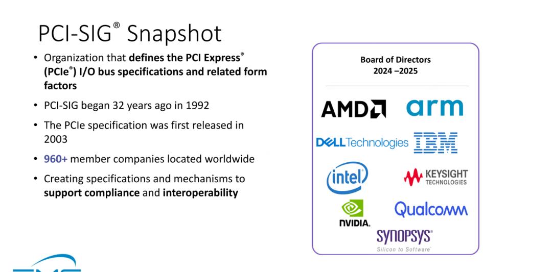
Image source: FMS
As the core interconnection technology of modern computing platforms, PCIe has comprehensively revolutionized the traditional PCI parallel bus with its serial bus architecture. Compared with the parallel transmission mode, PCIe has broken through the limitations of traditional technologies through three core characteristics:
Serial communication mechanism: Replacing the parallel architecture with serial transmission, it reduces signal interference at the physical layer and significantly improves data transfer efficiency and effective distance;
Point-to-point connection design: Each peripheral device is directly connected to the root complex through an independent link, eliminating the bottleneck of bus competition and realizing the directness and efficiency of data transfer;
Scalable bandwidth capability: It supports linear bandwidth expansion through the number of lanes, flexibly matching the performance requirements of different devices.
These technological characteristics not only provide far higher transfer bandwidth and lower latency for peripherals such as graphics cards, storage devices, and network cards than the traditional PCI but also reduce system occupancy through efficient resource scheduling, becoming the core technological foundation supporting the high-speed interconnection of contemporary computer hardware and profoundly influencing the architecture design and performance optimization direction of the entire computing system.
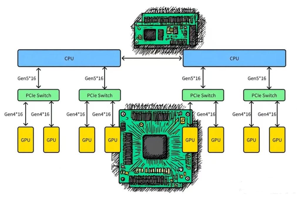
Image source: Xinwei Intelligent Computing
With the continuous development and application of PCIe technology, it has undergone multiple generations of iterative upgrades and has become the core technology for modern computer hardware interconnection, precisely meeting the continuously growing bandwidth requirements of contemporary computing platforms. As of December 2024, the number of its member companies has reached 1000.
20 Years of Rate Surge: The Iteration Path from PCIe 1.0 to 8.0
Since the release of the first version in 2003, PCIe has been upgraded from the initial 1.0 to 8.0, experiencing several important iterations, and the data transfer rate and performance have been continuously improved.
First, let's introduce the evolution history of the PCIe standard and the main differences between each generation of PCIe standards:
PCIe 1.0:
The Starting Point of Serial Interconnection, 2.5 GT/s Initiates the Bus Revolution
As the first standard of PCI Express technology, PCIe 1.0 was officially launched by PCI-SIG in 2003, marking the transformation from the traditional PCI bus to the serial interconnection architecture.
The single-lane transfer rate of PCIe 1.0 is 2.5 GT/s, using 8b/10b encoding, and the single-lane bandwidth is about 250 MB/s. Compared with the parallel PCI bus, PCIe 1.0 significantly reduces signal interference and improves the stability and efficiency of data transfer through the point-to-point serial link design. This bandwidth far exceeds that of PCI, and the speed of the bus has been significantly improved.
The PCIe 1.1 version launched in 2005 clarified and optimized the specification details without changing the core rate, laying a compatibility foundation for subsequent iterations and becoming the mainstream connection standard for early peripherals such as graphics cards and network cards.
PCIe 2.0: Rate Doubling and Compatibility Continuation
With the advancement of technology, PCIe 2.0 was officially released in early 2007.
PCIe 2.0 has achieved a leapfrog improvement in transfer performance on the basis of PCIe 1.x. The rate per lane has doubled from 2.5 GT/s to 5 GT/s, and the single-lane bandwidth has increased to 500 MB/s. The total throughput in the x16 configuration reaches 8 GB/s.
The PCIe 2.0 standard continues the serial link architecture in technology. By optimizing the signal integrity design (such as enhancing the pre-emphasis at the transmitter), it maintains full backward compatibility with previous-generation devices while meeting the increasing bandwidth requirements of peripherals such as high-definition graphics cards and high-speed storage.
The popularization of this version has promoted the hardware upgrade in the consumer electronics and server fields, becoming a key node for PCIe technology to move from its infancy to maturity.
PCIe 3.0:
CTLE Technology Paves the Way for High-Performance Graphics Cards and SSDs
In November 2010, the long-delayed PCIe 3.0 standard was officially released, marking that PCIe technology has entered a new stage of efficient transfer. This version achieves a transfer rate of 8 GT/s per lane, and the single-lane bandwidth has increased to about 1 GB/s. At the same time, it begins to use a more efficient 128b/130b encoding scheme to optimize transfer efficiency and maintains full compatibility with PCIe 2.0 in software and mechanical interfaces.
To support the high-frequency transfer requirements, PCIe 3.0 introduces advanced signal processing technologies such as continuous-time linear equalization (CTLE) at the receiver end. Combined with the transmitter de-emphasis mechanism and receiver equalization design, it effectively compensates for high-frequency signal attenuation and significantly improves signal integrity. In addition, it reduces transfer latency through protocol stack optimization and upgrades the power management mechanism to achieve refined power consumption control, meeting the energy efficiency requirements of both mobile devices and data centers.
As the mainstream interconnection standard for consumer and enterprise-level hardware in the 2010s, PCIe 3.0 provides sufficient bandwidth support for devices such as high-performance graphics cards and SSDs, promoting the overall leap in the performance of computing platforms.
PCIe 4.0: Unlocking the Full-Speed Potential of NVMe SSDs, Promoting Popularization in the Consumer Market
In 2017, the PCIe 4.0 standard came out, doubling the transfer rate again. The rate per lane reaches 16 GT/s, and the single-lane bandwidth is about 2 GB/s. The encoding scheme continues the efficient 128b/130b format. At the same time, it continues the idea of signal integrity optimization of the previous generation in technology. Through the enhanced equalization algorithm and clock synchronization mechanism, combined with the design of expanding the channel range with a timer, it effectively optimizes the stability of long-distance signal transfer and provides core support for the reliability of the link at high speeds.
As the first PCIe version that fully supports the full-speed operation of NVMe SSDs, the high-bandwidth capability of PCIe 4.0 significantly releases the storage performance potential and provides key support for the high-bandwidth requirements of scenarios such as high-performance computing and AI acceleration in data centers. This standard was first widely adopted by AMD's Ryzen 3000 series CPUs. With full backward compatibility with previous-generation devices, it achieved a smooth transition and quickly promoted its popularization in the consumer and enterprise-level markets, becoming the core interconnection standard for connecting high-speed peripherals such as SSDs and GPUs.
PCIe 5.0:
Three Technological Innovations, Continuous Improvement of Core Performance
Since the release of PCIe 4.0, the pace of technological iteration has significantly accelerated.
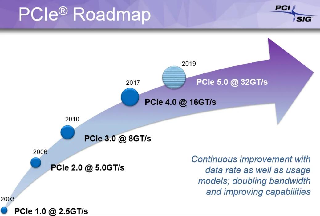
Image source: PCI-SIG
PCI-SIG officially released the PCIe 5.0 specification in May 2019. On the basis of maintaining backward compatibility with previous-generation technologies, it has doubled the transfer rate to 32 GT/s, and the single-lane bandwidth has increased to about 4 GB/s. Through the x16 configuration, it can achieve a throughput of 128 GB/s, which is sufficient to support the high-speed transfer requirements of 400GE networks in data centers.
As an extended upgrade of PCIe 4.0, PCIe 5.0 continues the mature technological framework, using the same Tx/Rx test method as the previous generation and the receiver stress jitter calibration mechanism based on the "eye" width and height. It only achieves a performance leap through targeted electrical optimization.
The core technological innovations of PCIe 5.0 are reflected in three aspects:
A new equalization bypass mode is added, supporting direct link training switching from 2.5 GT/s to 32 GT/s, significantly shortening the device initialization time and providing an efficient path for high-speed link equalization testing;
Through the optimization of channel margin adjustment and signal equalization technology, it effectively reduces signal loss in long-distance transfer and improves link stability;
While increasing the rate, it reduces latency. Combined with low-power design, it perfectly meets the performance requirements of data-intensive workloads such as artificial intelligence and machine learning.
Overall, the specification evolution of PCIe 5.0 focuses on core performance improvement and only makes targeted adjustments in key areas such as signal integrity enhancement and high-speed transfer support, achieving a leapfrog improvement in transfer efficiency with minimal technological changes.
PCIe 6.0: Redefining the Boundary of Data Transfer Efficiency
In January 2022, PCI-SIG officially released the PCIe 6.0 specification, marking that high-speed interconnection technology has entered a new development stage.
As a milestone version in the evolution of PCIe technology, PCIe 6.0 introduces pulse amplitude modulation PAM4 signal encoding for the first time. Without changing the channel bandwidth, it has achieved a doubling breakthrough in the transfer rate. The single-lane data rate has increased to 64 GT/s, and the corresponding single-lane bandwidth reaches 8 GB/s. Through the x16 configuration, it can provide a total throughput of 256 GB/s, which is sufficient to support the high-speed transfer requirements of 800GE networks in data centers.
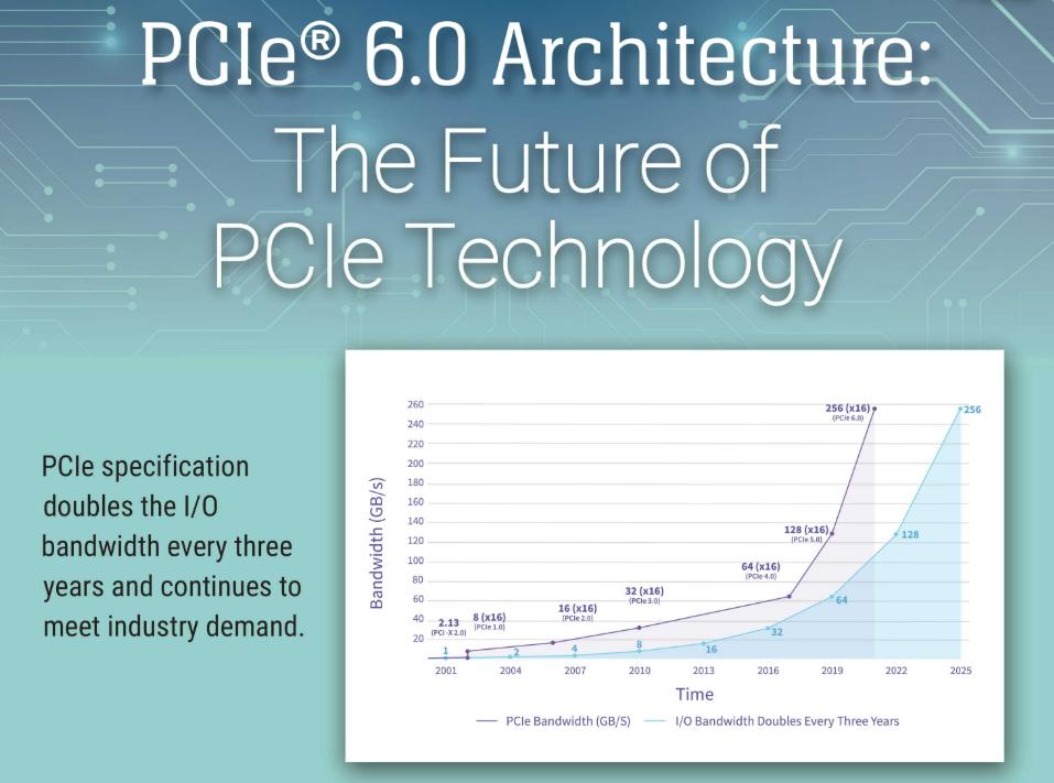
Image source: PCI-SIG official website
The core technological innovations of PCIe 6.0 are reflected in the multi-dimensional optimization of physical layer upgrade, logical layer innovation, and compatibility and reliability:
Physical layer upgrade: Replacing the traditional NRZ encoding with PAM4 modulation technology, it doubles the bandwidth at the same symbol rate through four-level signal transfer. At the same time, it introduces the forward error correction (FEC) mechanism to effectively compensate for signal loss in high-speed transfer and ensure data integrity;
Logical layer innovation: Introducing the flow control unit (FLIT) encoding, it encapsulates data into fixed-size 256B transfer units, replacing the 128B/130B encoding and DLLP overhead of the previous generation and significantly improving the transfer efficiency of transaction layer packets (TLP);
Compatibility and reliability: Continuing the backward compatibility design, while optimizing through technologies such as Retimer signal reconstruction and dynamic link equalization adjustment, it reduces latency while increasing the rate and ensures efficient communication of multiple devices in a tree topology.
These technological upgrades make PCIe 6.0 perfectly suitable for the high-bandwidth requirements of emerging scenarios such as AI training, machine learning, cloud computing, and hyperscale data centers, providing core support for the development of fields such as 5G, high-end storage, and visual computing.
As a technological revolution that reshapes the rules of hardware communication, PCIe 6.0 further consolidates its core position in computer system interconnection with a high-speed performance of 64 GT/s and redefines the efficiency boundary of data transfer between hardware devices.
PCIe 7.0: Breaking Through Transfer Limitations with Optical Retimers
In 2024, the PCI-SIG organization announced the PCIe 7.0 standard.
PCIe 7.0 continues the path of performance leap of previous generations. On the basis of PCIe 6.0, it doubles the bandwidth. The transfer rate per lane increases to 128 GT/s, and the bidirectional bandwidth of the x16 channel can reach 512 GB/s. The single-lane bandwidth is about 16 GB/s, further meeting the extreme performance requirements of data centers and AI applications.
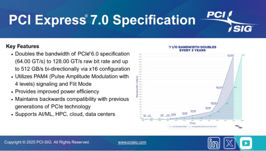
Image source: PCI-SIG official website
Technologically, PCIe 7.0 uses the PAM4 modulation and 1b/1b encoding scheme in the FLIT mode of PCIe 6.0 and maintains downward compatibility with previous-generation standards.
According to the PCI-SIG plan, this standard will focus on optimizing channel parameters and energy efficiency levels during the draft stage. The official specification will be completed in 2025, and the pre-release