AWS takes the easy way out, can the assembled networking perform well?
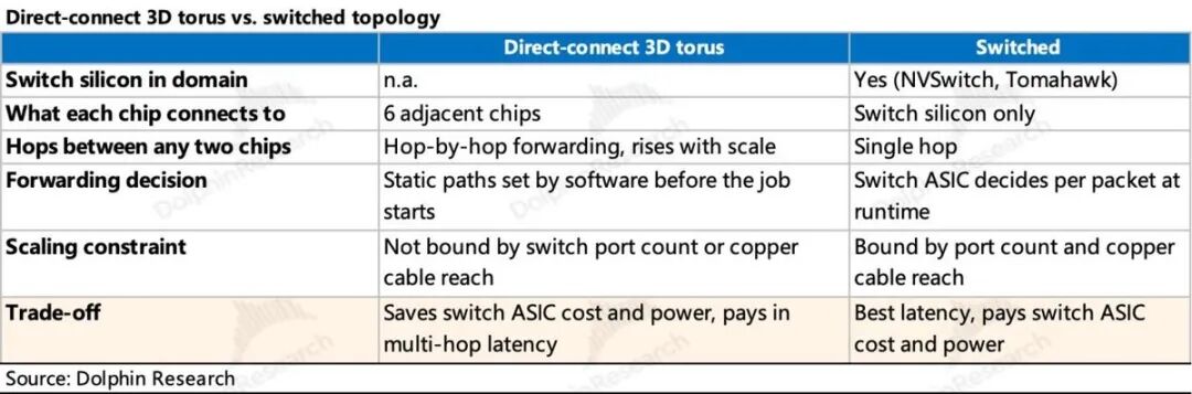
In recent series of networking analyses, Dolphin has sorted out the 2D fat-tree switched networking represented by NVIDIA & AMD, as well as the 3D torus direct-connect networking represented by Google.
NVIDIA is the industry benchmark. It independently develops the full stack of hardware, protocols and software, and the collaboration of software and hardware brings the best performance; the solution iterates fast with large spans, and the industrial chain logic also switches rapidly accordingly.
AMD follows NVIDIA's path but competes across generations. The Helios directly copies the networking architecture of GB300 NVL72, but its bandwidth performance targets Vera Rubin; key hardware such as switching chips still relies on external procurement. Although the Scale-Up bandwidth has caught up, the overall performance and cost still lag behind NVIDIA.
Google takes a separate path. With its excellent software capabilities, Google uses a 3D torus topology to connect nearly 10,000 Scale-Up domains through OCS, bringing cost-effectiveness under the demand of large-scale networking.
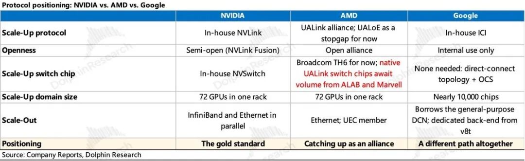
So, what about manufacturers that do not yet have strong competitiveness but are striving to supplement system-level delivery capabilities, especially networking capabilities? How do they operate?
This article turns to the last CSP giant with a system-level solution, AWS. The core feature of its networking is: launch first, then make up for shortcomings, buy instead of self-develop where possible, and choose cost-effective options. In other words, AWS is the company that does the least self-development across the entire industry.
Next, based on the above characteristics, Dolphin will dig deeper:
1. Can standard networking protocols work?
2. Networking topology transformation: from 3D torus direct connection to switched solution
3. Where are the opportunities in the AWS industrial chain?
1. Can standard networking protocols work?
1. Scale-Up Protocol: NeuronLink, a "shelled" PCIe
1) It is claimed to be self-developed, but its foundation is PCIe
AWS has independently developed the inter-chip interconnection protocol NeuronLink (NL, benchmarking against NVLink) to support its self-developed computing power chip Trainium (hereinafter referred to as Trn, benchmarking against NVIDIA's GPU), but this protocol is essentially a shelled PCIe. The aggregated bidirectional bandwidth of NLv4 per card is 2,304 GB/s (officially disclosed as 2TB/s, vs NVLink 6 & UALoE 3.6TB/s), and its evolution is as follows:

Also based on standard communication protocols, it is easy to associate that AMD has to adopt the UALoE (UALink over Ethernet, Ethernet-based) protocol as a transitional solution because its native UALink switching chip is still under development.
However, AWS has no intention of independently developing switching chips, so it is unlikely to break away from PCIe, because self-developed protocols usually need chip support. Later, it may instead become a purchaser of UALink, which will be expanded in the following networking solutions.
2) For the self-developed protocol, what exactly has been self-developed?
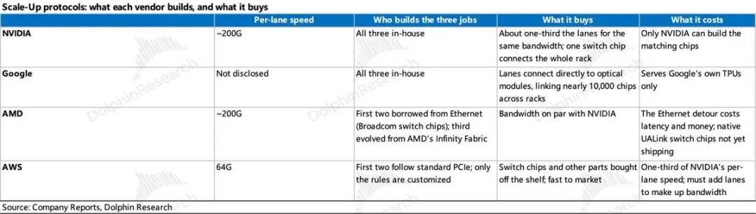
The industry seems to default that Scale-Up protocols must be self-developed to achieve high bandwidth and low latency. To judge whether AWS's PCIe-based networking protocol is good or not, we first need to understand what exactly each manufacturer has self-developed for their Scale-Up protocols. In short, a set of Scale-Up protocols needs to solve three problems:
a. How fast can the line run: Data is transmitted between chips through individual lanes (a pair of transmit and receive lines, which can be understood as a traffic lane). The speed of each lane depends on the performance of the SerDes circuit responsible for sending and receiving signals on the chip, which has the highest technical threshold.
b. What to do if transmission errors occur: Errors are inevitable on the line, and the protocol needs to specify how to detect errors and how to remedy them.
c. What operations can be performed between chips: That is, whether you can directly read and write data on the other side by address, just like accessing your own memory. The difference between Scale-Up and Scale-Out is defined at this layer.
Among the above three points, point a is the most important. Because points b and c are similar to defining rules, while the performance of the circuit is a problem of physical implementation, which is directly reflected in the per-lane rate. NVIDIA independently develops 200G SerDes, and AMD purchases Broadcom TH6 to also achieve 200G rate. The faster the per-lane speed, the fewer lanes are needed for the same bandwidth.
Back to AWS, the per-lane rate of PCIe Gen6 is only 64G. To make up for the bandwidth gap, either wait for PCIe iteration to increase the rate, or increase the number of lanes.
3) Is the PCIe-based communication protocol good? The answer is no
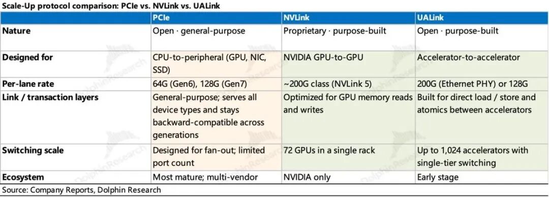
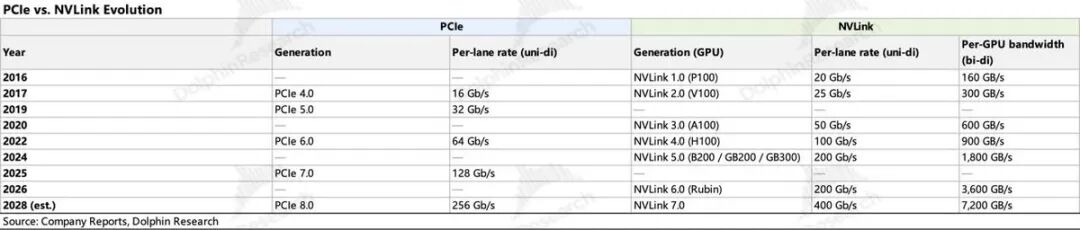
Even leaving aside AWS's solution, PCIe was originally designed for communication between CPUs and other devices (xPU, network cards, etc.). Compared with private protocols, in addition to the slow per-lane rate, it also has problems such as a limited number of ports, as detailed in the table below:
a. Wait for iteration to increase the rate?
The iteration pace lags behind. PCIe iterates approximately every three years, while NVLink iterates every two years. The iteration pace cannot keep up. In addition, it takes several years from the release of PCIe specifications to chip deployment, so AWS can only passively follow.
b. Is it feasible to increase the number of lanes?
The cost will rise sharply. To get more bandwidth between generations, you can only increase the number of lanes. But when the number of lanes increases, the cost of backplane copper cables, connectors and PCIe Retimers (used to solve the problem of signal attenuation on links) will rise accordingly, pushing up power consumption and overall cost.
c. Caught in a dilemma on both sides, why still choose PCIe?
The answer is simple: to save trouble and launch to the market quickly. AWS only needs to follow the standards at the protocol layer, and at the same time saves the R&D cycle of switching chips. For cloud vendors, they need to get rid of NVIDIA's premium to start independent development, and also need to meet the delivery requirements of computing nodes for anchor customers (Anthropic) as soon as possible, so they chose to use shelled PCIe. In other words, competitiveness is not their primary consideration, but deliverability is.
4) NLv5, UALink/NVLink may be a good destination
As for the next-generation protocol, if it is still based on PCIe Gen7, the situation of the protocol layer may be more embarrassing.
We can understand this from the evolution logic of PCIe. As shown in the table below, the per-lane rate from PCIe 5.0 to PCIe 6.0 has doubled by changing the modulation method.

There are two physical implementation methods to double the rate: one is to double the switching frequency of the signal (generated by high and low voltage switching), but the loss of copper wire increases sharply with the frequency, which puts very high requirements on the wiring; the other is to carry one more bit of information per signal switching.
The NRZ modulation method divides the voltage into two levels, high and low, transmitting 1 bit (i.e. 0, 1) per switching; the PAM4 modulation method divides the same voltage into four levels, transmitting 2 bits (i.e. 00, 01, 10, 11) per switching.
The problem with Gen 7 is that it can no longer double the rate by changing the modulation method, and can only increase the signal frequency, but the pressure on the board material and Retimer will rise exponentially, and the cost will get out of control.
Therefore, Dolphin believes that AWS has two ways out: first, when replacing the switching chip with UALink, the protocol layer will naturally adopt the UALink supported by the matching chip to achieve higher bandwidth; second, turn to NVLink — AWS has announced that Trn4 will support NVLink Fusion.
2. Scale-Out Protocol: The "lying flat" EFA
After looking at Scale-Up, AWS's networking strategy is roughly clear: it is very "Buddha-like" on Scale-Up where all manufacturers are fighting fiercely, and even more "lying flat" on Scale-Out, so we will only give a brief introduction here.
a. Bandwidth has not been improved for two generations. The Scale-Out layer is carried by AWS's self-developed EFA network, which is actually a variant of standard Ethernet. The Scale-Out bandwidth per card of the two generations of mainstream rack solutions is 200Gb/s with no improvement. For comparison, in the same period, NVIDIA increased from 800G of GB300 to 1.6T of Vera Rubin, and Google increased from 100G of v7 to 400G of v8t.
b. The Scale-Up domain is small, but the bandwidth is even lower. Google's nearly 10,000-card Scale-Up domain reduces the demand for Scale-Out, but still increases the bandwidth by 4 times; NVIDIA's domain has only 72 cards, and a large amount of traffic has to go through Scale-Out, so the bandwidth requirement of the network card is higher. AWS's Scale-Up domain has 144 cards, which is in the middle, but the Scale-Out bandwidth is only 200G, which is even lower than Google's.
c. The key switching hardware, the switching ASIC, is purchased externally. Although AWS independently develops the Nitro network card and white-box switches, the switching chips in them are purchased from multiple vendors (Broadcom, Marvell).

2. Networking Topology Transformation: From the Google Camp to the NVIDIA Camp
Starting from Trn3, AWS's networking route has switched. Trn2 has no switching chips, and uses 3D torus for point-to-point direct connection with copper cables (Google's solution is optical fiber + OCS), with a Scale-Up domain of 64 cards; Trn3 introduces switching chips, expanding the domain to 144 cards, and the number of hops between any two cards (each time data is forwarded counts as one hop) no longer increases with the scale. In other words, AWS has shifted from Google's direct connection route to NVIDIA's NVL72 switched route.
A natural question arises: Google can achieve direct connection for nearly 10,000 cards, why doesn't AWS continue to follow this path? The answer is that AWS's 3D torus is "pieced together", and it lacks the conditions that Google has to scale it up.
1. Trn2: The "pieced together" 3D Torus
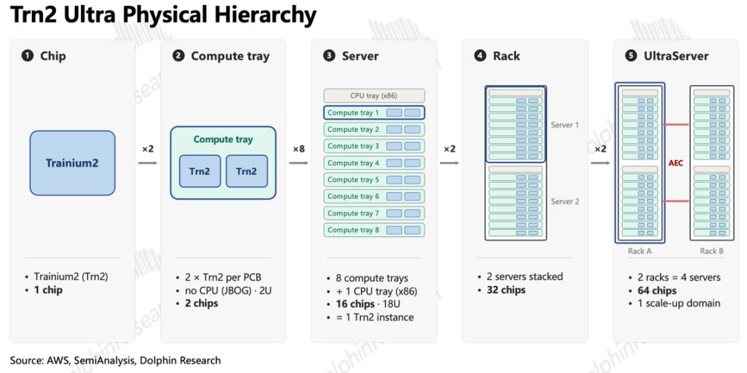
The old model Trn2 is no longer AWS's main push model, and we will give a brief introduction. Taking the rack-level solution Trn2-Ultra (there is also a regular 16-card Trn2 SKU in the same generation) as an example, the physical specifications from the inside out are shown in the following figure.
1) How is the 2D torus connected?
a. Intra-Tray: Each computing tray is equipped with 2 Trn2 cards, the two cards are directly connected through PCB traces (orange dotted line in the figure);
b. Intra-Server: 8 computing trays and 1 CPU tray form a 16-card server, the computing trays are connected through the backplane copper cable at the rear edge of the chassis, and the computing tray and the CPU tray are connected through the front panel via DAC (passive copper cable).
Topology: 16 cards are connected in a 4×4 layout, each row is composed of 2 trays, each column spans 4 trays, and each row and each column are connected end to end to form a ring (which is exactly the meaning of