After the price of a layer of "cloth" has surged by 270%, investment institutions have bet hundreds of millions of yuan on the glass substrate track, and Xunlin Technology has completed a Series B financing of nearly 200 million yuan.
[Introduction] At present, the price of electronic-grade fiberglass fabric has doubled compared with the low point in 2025, the price of FR-4 copper clad laminate has increased by more than 270%, the delivery lead time of some AI packaging substrates has been extended to more than 6 months, and the supply crisis of organic substrates continues to deepen. Against this backdrop, Xunlin Technology, a leading domestic glass substrate enterprise, announced the completion of Series B financing of nearly 200 million yuan — which is already the third round of financing completed by the company within half a year. This round of financing is led by new shareholders including Inno Fund, Qiancheng Capital, Hymson, Prolight, and Tongxin Capital, while existing shareholders such as Jinyu Maowu, Haitong Kaiyuan, and Beishan Industrial Investment continue to increase their investment. The raised funds will be mainly used for glass substrate capacity expansion, packaging production line construction and operation, process precision upgrading R&D, and cutting-edge optical communication application layout.
Shareholding Structure: Market-oriented Capital, Industrial Capital and Regional State-owned Capital Gather, Existing Shareholders Make Additional Investments
The shareholder lineup of this round presents a distinct "trilogy": market-oriented hard technology funds represented by Inno Fund, Qiancheng Capital and Tongxin Capital, which have long been deeply engaged in the semiconductor and advanced manufacturing sectors; industrial capital represented by Hymson and Prolight, which come from the laser equipment and optical communication industries respectively, the two upstream and downstream sectors strongly related to glass substrates; market-oriented funds, regional state-owned capital and securities firm-backed capital represented by Jinyu Maowu, Beishan Industrial Investment and Haitong Kaiyuan, continue to increase their investment in this round. The continuous investment from diverse shareholders provides solid support for the company's industrialization process, and is also the most direct confirmation of its mass production progress.
Industry Background: Overlay of Substrate Shortage and Price Hike Wave Creates a Definite Window for Glass Substrates
This round of financing is essentially a strategic stake-taking at a favorable time window. With the rapid surge of AI computing power, packaging substrates are in continuous shortage, ABF substrates are in short supply and their delivery lead time is repeatedly extended; as chip packaging sizes continue to break through and optical module rates keep rising, organic substrates are approaching their physical limits in terms of thermal expansion matching, high-frequency loss and wiring density. The choices of industry giants have already given the answer: Intel announced that its Glass Core Substrate (GCS) has entered large-scale mass production, TSMC's CoPoS trial production line will be put into operation within the year, and Samsung and SKC Absolics are accelerating sample delivery and mass production preparation. Glass substrates are moving from the laboratories of giants to the center of the industry.
Core Logic of Substitution: One Layer of "Fabric" Restricts Organic Substrates, Three Major Applications Are Fully Shifting to Glass-based Solutions
What is more noteworthy than the moves of industry giants is that the cost foundation of organic substrates is being loosened. Since the second half of 2025, the PCB industry chain has experienced a rare round of price hikes: the price of copper clad laminates has risen sharply, and all PCB manufacturers have raised their prices across the board. The real source of the price increase is neither copper foil nor resin, but a layer of "fabric" — electronic-grade fiberglass fabric. Its price has doubled compared with the low point in 2025, the industry inventory has dropped to an extremely low level in history, high-end low-dielectric products are highly monopolized by overseas manufacturers, and capacity expansion takes years to complete. The shortage of this layer of "fabric" has no solution in the short term.
The reason why fiberglass fabric is indispensable is that it is the "skeleton" of organic substrates, and one of its core missions is thermal stress matching: as the number of layers of AI server PCBs continues to rise, in order to make the thermal expansion coefficient of organic base materials close to that of silicon chips, the industry has to use a large amount of expensive low-CTE special fiberglass fabric. In other words, organic substrates are using increasingly expensive "fabric" to imitate the inherent properties of glass — glass has a natural CTE matching silicon, its dielectric loss is much lower than that of organic materials, and it does not need this layer of "fabric" at all. When the cost of this "patch" crosses the inflection point of material substitution cost, glass-based development changes from an optional item to an inevitable trend. But "glass-based transformation" is not a single thing, but three things — the demand logic, technical indicators and industrial rhythm of the three major applications are completely different:
The first category, PCB substitution — stock substitution driven by economic efficiency, with the fastest rhythm. Targeting AI server backplanes, high-frequency communication boards and new display substrates, the substitution targets are FR-4 and traditional PCBs, with a simple and sharp logic: better performance and lower cost. The signal loss is significantly reduced, and the comprehensive cost in display and HDI substrate scenarios is much better than that of PCB substrates. This category focuses on large-scale manufacturing and cost control capabilities, and is the main battlefield for current volume growth — 2026 will be the first year of glass-based PCB substitution.
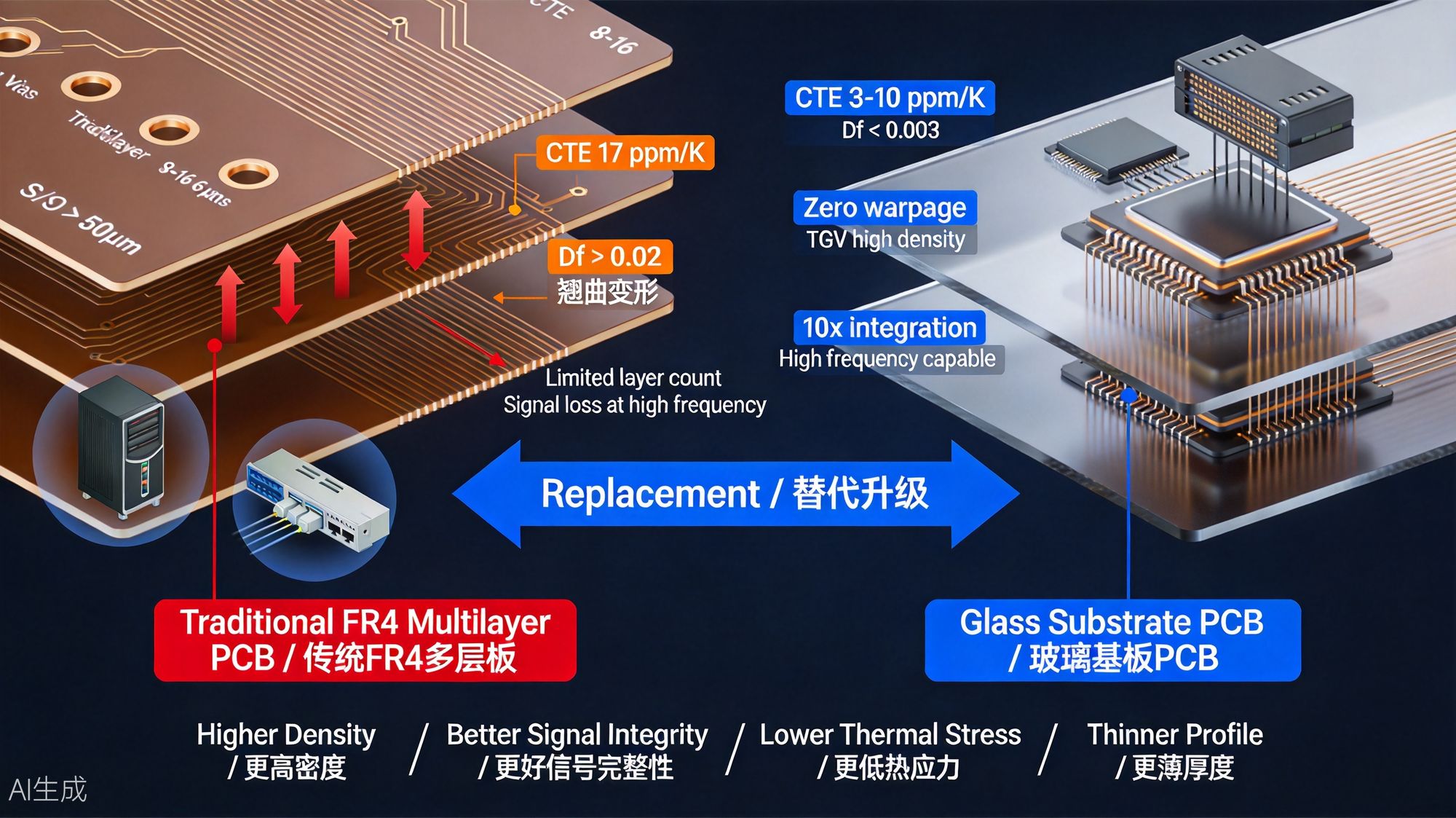
Schematic Diagram of Glass Substrate Substituting Traditional PCB
The second category, ABF substrate substitution — driven by reliability and supply security, with a moderate rhythm. Targeting ultra-large-size FC-BGA packaging, Chiplet and HBM high-bandwidth memory, it replaces substrates that are monopolized by overseas players and in continuous shortage. This is a duel of strict technical indicators: warpage, line width and line spacing, aperture and aspect ratio are all comprehensively tightened, testing the in-depth capabilities of precision process and reliability verification. Related products will be gradually launched to the market in 2027.
The third category, Interposer substitution — long-term substitution driven by cost revolution, with the largest market space. Targeting CoWoS advanced packaging and CPO optoelectronic co-packaging, it replaces expensive silicon TSV interposers: glass has significantly better dielectric properties than silicon, higher panel-level processing utilization, and its comprehensive cost is expected to be much lower than that of silicon TSV; more importantly, in CPO scenarios, glass can directly carry optical waveguides to realize optoelectronic integration. This industrial chain will gradually mature from 2027 to 2030 — whoever takes the position in advance will hold the admission ticket for next-generation packaging.
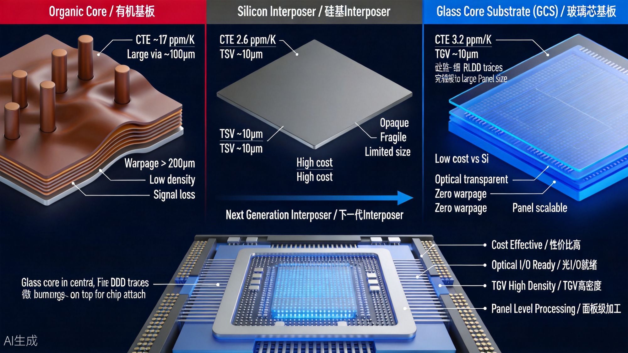
Schematic Diagram of Application of Glass Core Substrate and Glass Interposer
It is worth noting that when the industry generally focuses on GCS (Glass Core Substrate) and GI (Glass Interposer), the glass-based transformation of PCB will also inevitably be implemented rapidly, but Glass PCB has a harsh prerequisite: the substitution indicators are extremely high, and very few enterprises can truly meet the requirements. To replace organic PCBs, glass substrates must cross three thresholds at the same time — cost framework, the TGV substrate cost model of most enterprises cannot be closed at all; high copper thickness to line width ratio, under fine circuits, high current driving for server power supply and display also requires thick copper, while thick copper is just a common shortboard in the glass copper cladding process of the industry; full-process direct yield, which is the industry-recognized lifeline for economic efficiency, and the domestic mass production level varies unevenly. Xunlin Technology is one of the very few enterprises in the world that have passed all three indicators and have the possibility of mass production: its comprehensive cost is expected to be significantly lower than that of similar PCBs, it has both thick copper capability and fine circuit performance, its direct yield leads the industry, and its copper cladding bonding strength is several times higher than the industry average, which ensures the long-term reliability of mounting and rework. In the window of continuous price hikes, the cost-performance balance between glass substrates and organic PCBs is reversing — and enterprises that can meet the demand after the reversal must first pass these three barriers.
Mass Production Progress: The Last Mile Has Been Opened Up
The industry never lacks concepts and samples, what it lacks is real production capacity that can achieve stable batch delivery. From the perspective of Xunlin Technology, only when the factory is put into operation, the yield is verified, and the cost model is closed, can the demand change from sample orders to sustainable batch orders. To this end, Xunlin has independently built a full-process glass substrate factory in Tianjin, covering the entire process from cutting, thinning, TGV pore forming, to PVD metallization, electroplating, patterning, and solder mask, with an annual production capacity of 300,000 square meters. Relying on self-developed PVD copper cladding technology derived from aero-engine thermal barrier coating systems and Cu-ABX quaternary alloy seed layers, the company's copper cladding bonding strength is several times higher than the industry level, the mass production aperture and aspect ratio of TGV cover mainstream demands, and the continuous VCP electroplating capacity is several times that of traditional lines. At present, the company's Mini LED backlight, COB direct display and MIP display module substrates have entered the batch shipment stage, and have passed the verification of leading domestic customers through its own module packaging lines — the "last mile" for glass substrate PCBs to move from the laboratory to the production line has been opened up.
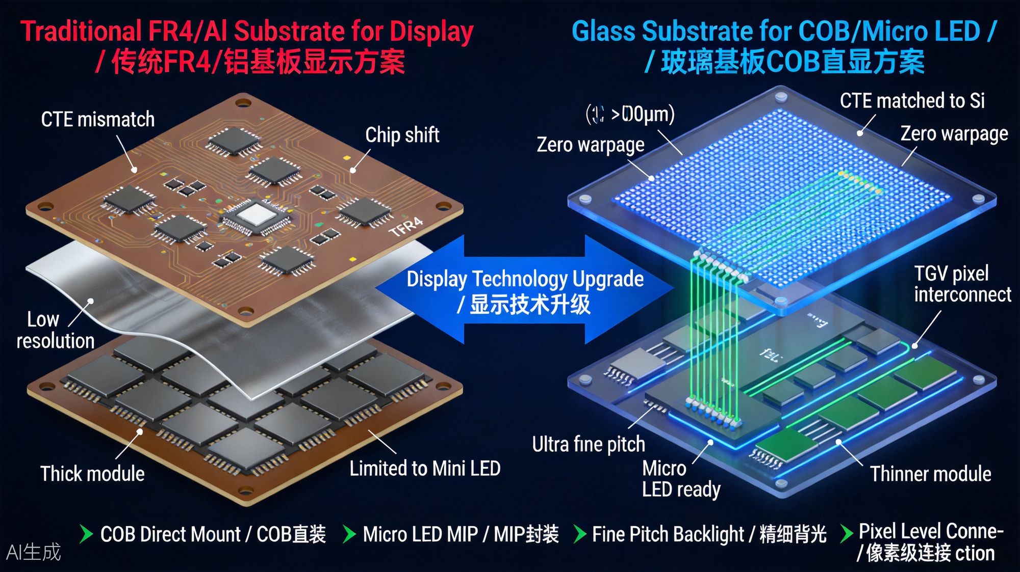
Application of Glass Substrates in MicroLED
Processing Path: Three Sets of Process Platforms Progressively Interact, Six Levels of Precision Realize Gradual Leap
The logic of Xunlin's capacity expansion is not simple replication of production capacity, but to build three progressive and interactive process platforms around underlying capabilities such as TGV pore forming, PVD metallization, electroplating and patterning, to gradually tighten indicators in five dimensions: aperture, pore density, structure, number of layers, line width and line spacing, and gradually expand the market — six levels of products move up step by step along three main process lines.
The starting point of this path is the first platform — large-size glass-based PCB process centered on subtractive method: the display backlight and COB glass-based PCB that have entered mass production, with double-sided copper cladding and TGV vertical conduction, large panel size and high yield, are not only the basic cash flow source, but also the reliability base for all levels; by tightening the patterning precision on the same platform, it extends to glass-based HDI, introduces micropores and buried blind holes, realizes multi-layer TGV fine wiring, and enters the high-speed PCB and optical module substrate market. The second platform is high-level interconnection process centered on semi-additive fine circuits and multi-layer bonding: high-level HDI realizes multi-layer stacking through unit body bonding, avoiding the cumulative alignment error of layer-by-layer lamination, which is Xunlin's differentiated approach for multi-layer development; this fine circuit capability continues to extend to substrates, opening up the GCS glass core substrate market — shifting to the fine process of "via — via filling — RDL — multi-layer stacking", directly targeting the tens of billions of dollars ABF stock substitution market, which is also the main R&D direction of this round of financing. The third platform is oriented to the integration of packaging and optics: high-precision TGV and glass interposer (GI) continue to tackle key problems in smaller aperture, higher aspect ratio and higher via density, with cost expected to be much lower than silicon TSV, targeting the long-term market of 2.5D/3D packaging and HBM; by adding optical processing capability on the same platform, ion-exchange optical waveguide, laser direct writing modification, optical fiber through-hole and precision cavity are processed on the same board, and finally the co-construction of "circuit + optical path" on the same board is realized. The three sets of platforms are not isolated from each other: the copper cladding reliability and mass production yield verified by the subtractive method platform are the common foundation for fine circuit and packaging processes; the precision capabilities accumulated in via filling, RDL and optical processing in turn continuously support the precision improvement of the first two platforms — they are mutually supportive in the progressive development.
This six-level path is not a jump-style bet, but a linear evolution of precision iteration — which is completely isomorphic with the climbing logic of large domestic PCB manufacturers of "single/double panel — multi-layer board — HDI — high-level HDI — IC substrate": the aperture is continuously tightened, the circuits are getting finer, and the number of layers develops from double-sided to dozens of layers, which is essentially continuous narrowing and gradual superposition on the basis of shared underlying process capabilities. This model fundamentally avoids the biggest hidden risk in the industry — production line obsolescence and investment failure: core processes such as TGV, PVD, electroplating, exposure and etching are widely reused across the three platforms, platform upgrading relies on process package iteration and modular process superposition instead of rebuilding from scratch; the mass production revenue of each level of product in turn supports the R&D of next-generation products. The production capacity formed by this round of financing will not depreciate with product iteration, but will continue to appreciate as precision improves.
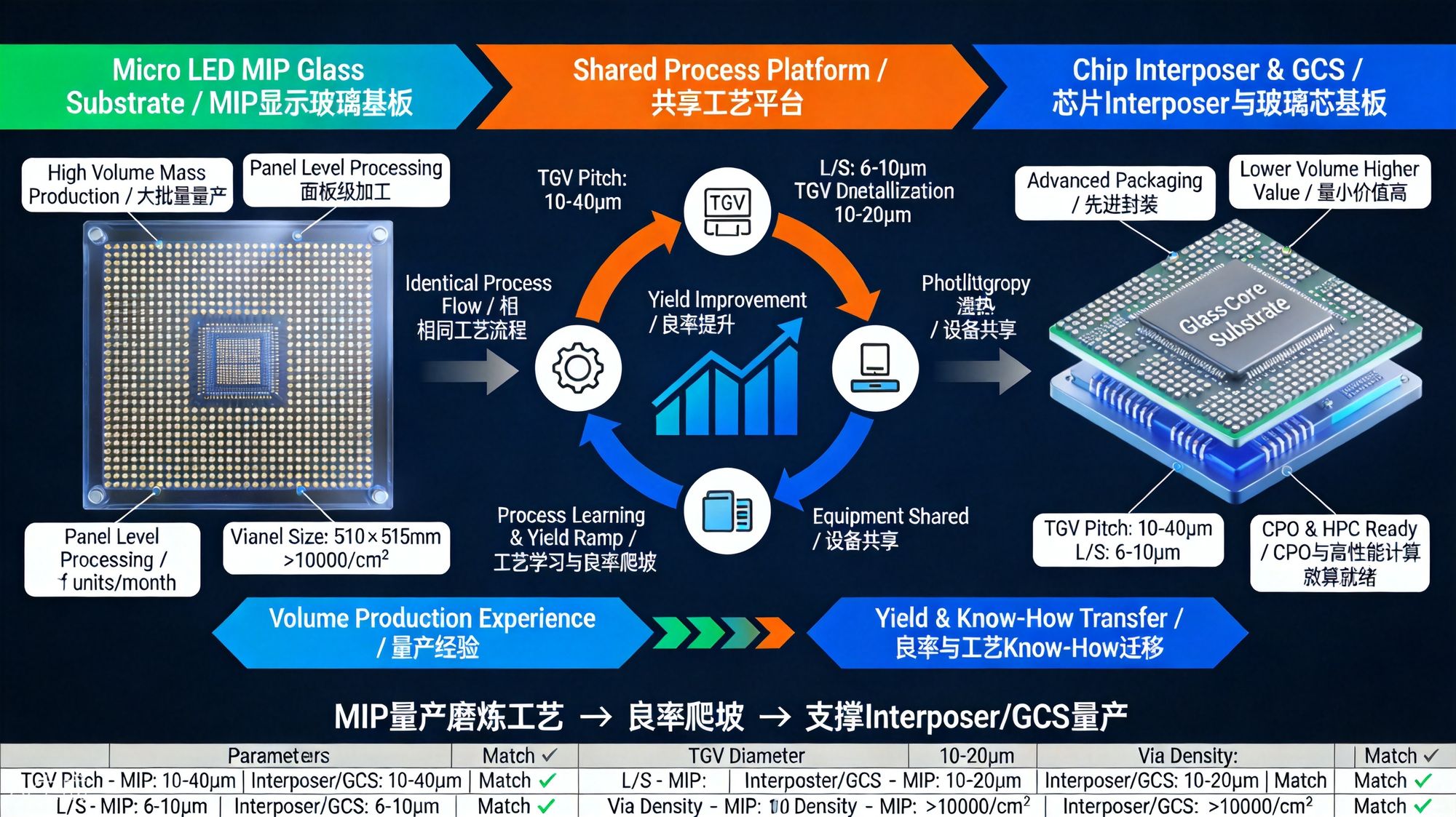
Logic of Industrial Upgrading and Transition of Glass Substrates
Views of Investors and Founders
The lead investor of this round, Inno Fund, stated: "Glass substrates are at a critical window shifting from technical verification to large-scale mass production. We value Xunlin Technology's original breakthroughs in underlying processes such as PVD copper cladding, and more value its capability of building a full-process production line and realizing batch shipment — in hard technology investment, teams that can deliver real results are the most scarce."
Dr. Zhen Zhen, Founder and CEO of Xunlin Technology, said: "This round of financing is the dual confirmation of the mass production route of glass substrates by industrial partners and market capital. The price hike of fiberglass fabric has made the whole industry see clearly the cost ceiling of organic substrates, and also made the substitution value of glass substrates have economic certainty for the first time. Next, the funds will be focused on capacity ramp-up, packaging implementation and precision upgrading — from display substrates to high-level HDI, from glass core substrates to optical waveguides, we use three sets of progressive and interactive process platforms and continuous precision leap to make real batch delivery the ultimate solution to industry demands."
About Xunlin Technology
Founded in September 2023, Xunlin Technology focuses on R&D and industrialization of full-process glass substrate technology, covering core processes such as TGV through-vias, PVD composite coating, continuous electroplating and fine circuits. Its products are applied in fields including Mini LED backlight, COB/Micro LED direct display, glass-based HDI, advanced packaging substrates and optoelectronic co-packaging. The company has realized mass production of Micro LED-level circuit precision and high-density TGV substrates, and is accelerating the expansion of its industrial territory from substrates to modules, from display to packaging, and from electricity to optics.