Advanced Packaging Steps into a New Battlefield
Recently, in the article Who Is Scrambling for CoWoS?, the author sorted out the fierce competition among global AI chip giants for CoWoS packaging capacity. From NVIDIA, AMD to Broadcom, MediaTek, and even the self-developed chip teams of cloud giants, all are frantically competing for TSMC's CoWoS capacity — the demand has surged from about 1.38 million wafers in 2026 to over 2.68 million wafers in 2027. It is clear that advanced packaging has become the core bargaining chip in the competition of the computing power industry.
Just as CoWoS is at its peak, a next-generation packaging technology designed to solve its deep-seated pain points and cater to the era of larger-sized chips — CoPoS — has quietly matured.
On July 18, at WAIC 2026, Enflame Technology, a leading domestic AI chip enterprise, and Shanghai Xianfeng Technology jointly released China's first CoPoS advanced packaging sample with glass substrate for AI computing chips, which for the first time deeply integrated domestically developed high-end AI computing chips with core domestic CoPoS advanced packaging technologies, drawing high attention from the industry.
On the other hand, TSMC, the absolute leader in advanced packaging, has long included CoPoS in its long-term technology blueprint, built a dedicated trial production line, and cooperated with the global supply chain to promote verification. TSMC's sharing at its corporate briefing has clearly outlined the complete timeline of CoPoS from trial production to mass production, which is regarded as the most crucial footnote for this technical route.
From CoWoS to CoPoS, there is only a one-letter difference, but it may mean a structural leap in the semiconductor packaging industry.
CoWoS is great, but not enough
To understand CoPoS, we need to start with CoWoS.
As we all know, CoWoS is the benchmark for 2.5D advanced packaging. The fundamental reason why it has become a "strategic spot that every military must fight for" is that it solves the integration problem of AI chips: GPU/CPU dies and HBM high-bandwidth memory are interconnected at high density through a silicon interposer, and packaged on a unified substrate of super-large size.
However, although this solution has excellent performance, its challenges are becoming increasingly prominent:
Soaring costs: The silicon interposer itself is expensive, accounting for more than half of the total packaging cost.
Limited size: Restricted by the size of 12-inch wafers, the maximum chip area it can support is capped. As AI chips become larger (for example, the area of NVIDIA B200 has exceeded 800mm²), cutting square chips on a circular wafer will cause serious area waste, with a material utilization rate of less than 70%.
Warpage risk: The coefficient of thermal expansion (CTE) between silicon chips and organic substrates is severely mismatched (silicon is about 2.7ppm/℃, organic substrate is about 16ppm/℃), which is very prone to warpage under large sizes and affects yield.
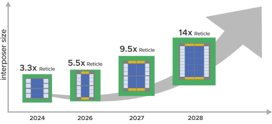
Image source: TSMC
CoPoS was born to solve these problems. Its full name is Chip-on-Panel-on-Substrate, which is a new generation of panel-level advanced packaging technology iterated based on the pain points of CoWoS. As the name suggests, the biggest difference between CoPoS and CoWoS is that the circular silicon wafer originally used as the interposer is replaced by a square panel.
In the CoWoS solution, chips are placed on the circular silicon interposer and then packaged on the substrate as a whole. CoPoS uses a large square panel as the carrier of the redistribution layer (RDL): chips are first placed on the panel, and then packaged on the final substrate after interconnection is completed.
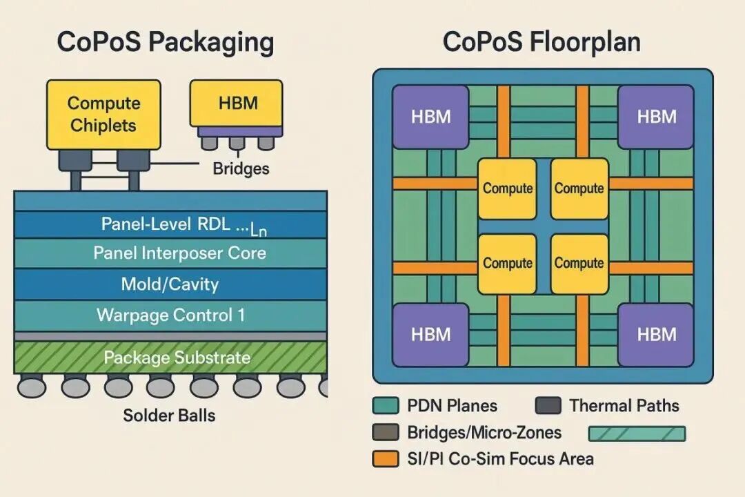
Schematic diagram of CoPoS packaging architecture
According to data from OpenRouter, the world's largest aggregated platform for AI model APIs, in the first half of 2026, the weekly Token call volume of AI models surged from 6.4 trillion in January to 46.7 trillion in July — an increase of more than 7 times in half a year.
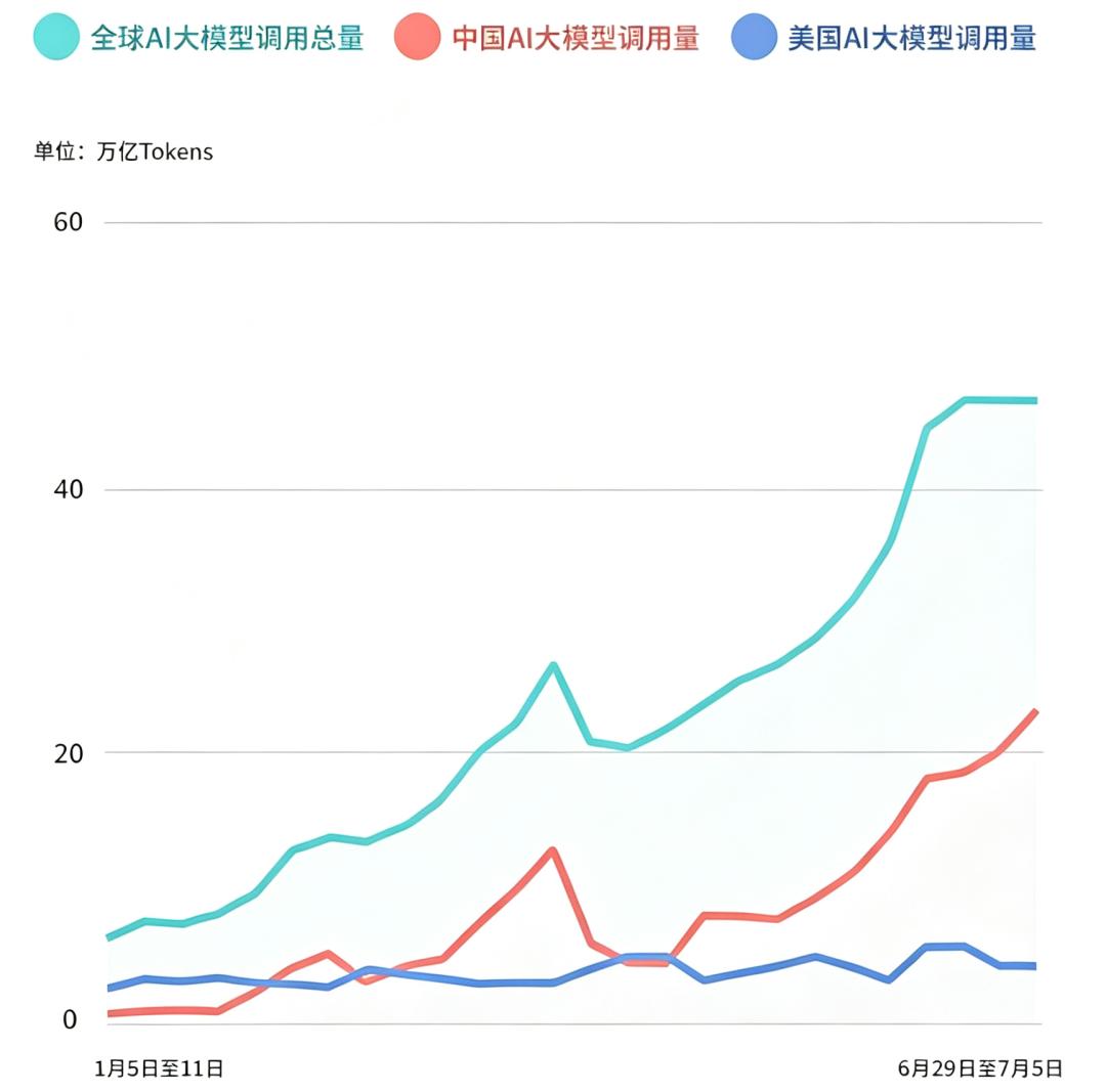
Image source: OpenRouter
Behind the surge in Token call volume is the extreme packaging demand of ultra-large-scale AI chips for "larger area, higher interconnection, and lower cost". When the chip packaging area jumps from 3.3x mask size to 9x, traditional wafer-level solutions can no longer meet the requirements. CoPoS panel-level high-density packaging is becoming a key path for the industry to break through the dual bottlenecks of performance and cost.
To use a vivid metaphor: CoWoS is like cutting rectangular pizza slices from a round pizza. No matter how you cut it, there will always be a lot of leftover scraps at the edge of the circle. CoPoS, by contrast, is to spread the pizza directly on a square baking tray, with almost no waste, and the output per unit area is greatly improved.
According to industry analysis, the core advantages of CoPoS over CoWoS are reflected in the following aspects:
Leapfrog improvement in area utilization
The effective area utilization rate of 12-inch circular wafers is about 70%, while the utilization rate of square panels can reach 95% or even higher. Taking a 510×515mm panel as an example, its effective area is about 4.5 times that of a 12-inch wafer. This means that on the same base plate, CoPoS can place more chips and HBM stacks, directly reducing the packaging cost per unit area. It is estimated that CoPoS can reduce the cost per unit area by 20%-30%.
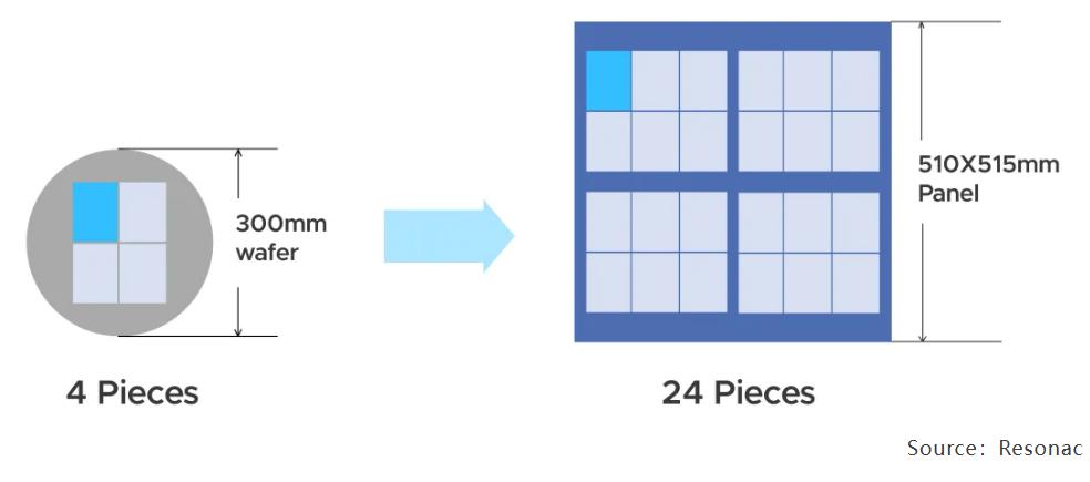
The upper limit of packaging size is greatly raised
Limited by the size of circular wafers, the maximum packaging size of CoWoS is currently about 5.5 times the mask area. After adopting square panels, CoPoS can support super-large packaging sizes of more than 9.5 times the mask area or even larger, leaving sufficient space for the further upgrading of next-generation AI chips, and is a key path to support multi-HBM stacking and Chiplet integration.
Fundamental breakthrough in production capacity bottlenecks
One of the core bottlenecks of the current tight CoWoS capacity is the physical limit of 12-inch wafers — the number of chips that can be produced from each wafer is limited, and the equipment capacity of wafer-level packaging is constrained. After shifting to panel-level packaging, not only the output of a single panel is several times that of a wafer, but more importantly, panel-level packaging can reuse or transform the existing production lines of the display panel industry (such as the fully depreciated large-generation panel production lines), providing a new path for rapid capacity expansion.
Natural advantages of glass substrates
The long-term evolution direction of CoPoS is the glass core substrate. Glass has inherent low warpage, high dimensional stability, excellent electrical insulation performance and finer wiring accuracy, which is especially suitable for high-frequency and high-speed signal transmission scenarios. The interconnection density is expected to reach 10 times that of organic substrates. Compared with organic substrates, glass substrates perform better in heat dissipation management and signal integrity of high-computing-power chips.
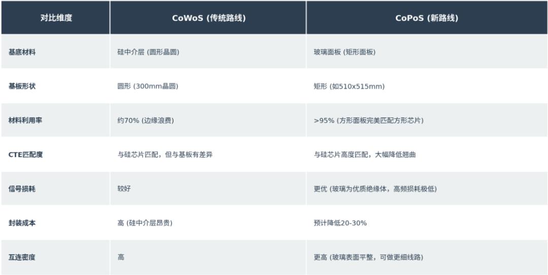
For the entire semiconductor industry chain, the emergence of CoPoS means that the packaging process has been upgraded from an auxiliary process of wafer fabs to an independent strategic highland, and panel manufacturers, packaging equipment vendors, and material suppliers will all embrace new growth curves.
CoPoS race: Who is seizing the position?
TSMC: A cautious and determined leader
As the absolute leader in the field of global advanced packaging, TSMC has the most systematic and in-depth layout of CoPoS.
It is understood that TSMC has built a CoPoS pilot line, entering the joint verification stage of equipment and processes, and has simultaneously launched multi-specification square panel solutions covering 310×310mm, 515×515mm, and 750×620mm. 2026 is the key verification period, trial production will start in 2027, and mass production will be launched in the second half of 2028.
As the industry weathervane, TSMC clarified the progress of CoPoS at a recent corporate briefing. Chairman Wei Zhejia said that CoWoS is still the mainstream, but TSMC is developing CoPoS as an "alternative solution" to reduce costs, and is cooperating with substrate suppliers. The key progress is that a trial production line is under construction, which is expected to take about 1 year to mature. In the second half of 2027, 510×515mm mass-production-specification panels will be used for joint customer verification, and then production can be put into operation. This is consistent with the previous plan of trial production in 2027 and mass production in the second half of 2028.
According to sources, the Chiayi AP7 plant is planned to be the core mass production base, which is scheduled to be completed in June 2026 and achieve large-scale capacity release from the end of 2028 to 2029; the Arizona advanced packaging plant in the United States is also equipped with a CoPoS production line, and it is planned to introduce CoPoS capacity in 2029-2030. At the same time, TSMC admitted that even if mass production starts in 2028, it will still take 2-3 years to form sufficient supply scale; the mass production time point of the complete CoPoS process integrated with the glass core substrate is scheduled for after 2030.
According to another DigiTimes report, TSMC has built a CoPoS trial production line in the Cypress Longtan plant, and a second trial production line is planned to be added in the Chiayi AP7 plant; the CoPoS mass production line in the US plant is also under construction at the same time.
In terms of capacity planning, TSMC's Taiwan plant is expected to achieve small-scale mass production in 2028, with a monthly output of no less than 500 Panel-specification CoPoS packaging products. Capacity expansion will be accelerated in 2029, and the monthly capacity will rise to 12,000 Panel by the end of the year. In 2030, the monthly capacity will increase by 241% year-on-year to 30,000 Panel; in 2031, the monthly capacity will increase by 177% year-on-year to 53,000 Panel.
Revealed by the supply chain, NVIDIA is expected to become the first customer of CoPoS, and its next-generation Feynman series GPUs have been included in the CoPoS adaptation plan. The first-generation products are expected to be equipped with 3D stacking and SiC carrier heat dissipation solutions in 2028; the Feynman Ultra version to be launched in 2029 is expected to fully implement the CoPoS packaging technology, using its larger packaging area to accommodate more GPU chiplets and memory.
In addition, AMD, Broadcom, Google HPC chips, etc. are also carrying out pre-technical docking at the same time, and existing CoWoS customers will switch to CoPoS in stages.
It can be seen that TSMC's involvement has given the strongest endorsement for CoPoS and driven the entire supply chain. According to media reports, the first batch of CoPoS equipment test prototypes have been stationed in TSMC's subsidiary Cypress Technology, and equipment vendors including Canon, DISCO, Applied Materials, and Lam Research have all seized positions and entered the verification stage.
However, according to DigiTimes, TSMC has implemented strict confidentiality control over the CoPoS supply chain, requiring local Taiwanese equipment and material partners to limit information sharing, and some technologies are expected to be exclusively used by TSMC for several years after mass production.
Analyst Ming-Chi Kuo also specially reminded the industry risk: the current substrate and equipment manufacturers participating in CoPoS verification are not the final mass production suppliers, and enterprises that only stay in the concept stage and do not participate in actual machine testing will most likely be reshuffled by the supply chain, and the industrial chain pattern will be reshaped with the completion of production line verification.
This "ecosystem locking" strategy aims to make CoPoS another competitive moat after CoWoS.
Domestic forces: Enflame Technology and Xianfeng Technology take the lead in "sprinting"
What surprises the industry most is the speed of domestic manufacturers.
On July 18, during WAIC, Enflame Technology jointly released China's first AI chip sample based on CoPoS technology with Xianfeng Technology. Enflame Technology claimed that its CoPoS solution is at least two quarters ahead of the mass production timetable of the same route announced by TSMC, marking that domestic advanced packaging has moved from the stage of "whether it exists" to the stage of "competition for speed".
According to the technical team of Xianfeng Technology, the packaging sample comprehensively applies a number of cutting-edge technologies: using the glass substrate as the core carrier, constructing a multi-layer metal interconnection structure through Physical Vapor Deposition (PVD) technology, and realizing micron-level circuit accuracy combined with panel-level lithography patterning technology; at the same time, precision electroplated build-up, chemically etched metal sacrificial layer, and panel-level RDL design are adopted to effectively improve signal transmission efficiency and packaging density.
It is worth noting that the R&D team has specially developed a warpage-controlled low-stress plastic packaging process for the heat dissipation and structural stability requirements of high-computing-power chips, optimized the heat conduction path through the insulating layer slit coating technology, and adopted micron-level mounting technology and surface grinding forming and cutting technology to ensure the long-term reliability of the chips in high-speed computing scenarios.
Industry experts pointed out that this sample has reached the international advanced level in key indicators such as signal integrity and power consumption control, and has passed a number of strict tests and verifications, with comprehensive performance meeting the packaging requirements of next-generation AI training chips.
The significance of this "sprint" is to verify the engineering feasibility of the domestic panel-level packaging industry chain, especially the fact that domestic packaging equipment can already support the requirements of AI chip level in terms of accuracy and stability. Although there is still a long way to go from sample to mass production, it sends a strong signal: at the starting line of the new generation of packaging technology, domestic enterprises are no longer just followers, but have the ability to run in parallel in stages or even take the lead in some local fields.
On the whole, CoPoS is no longer