Is the most expensive lithography machine no longer selling well?
Nowadays, High-NA EUV has crossed the technical verification threshold, but the attitudes of the three major fabs toward it have clearly diverged: Intel is sprinting ahead, TSMC is doing cost-benefit calculations, and Samsung is hitting the brakes. As things stand, the three paths are not about which one is more advanced, but which one has a greater need for High-NA.
Intel: A Process Validation That Cannot Be Afforded to Lose
In July 2026, ASML announced that Intel has used EXE-series High-NA EUV tools in specific Intel 18A process layers for some Panther Lake products and entered high-volume manufacturing. The relevant High-NA process layers have already achieved yields comparable to the traditional NXE low-NA EUV platform.
However, the entire Intel 18A process does not use High-NA; nor do all Panther Lake products use High-NA — only some products and some critical layers do. In other words, Intel is not using High-NA to fully replace Low-NA, but rather verifying exposure, overlay, equipment utilization, yield, and maintenance data in a real mass production environment.
Back in 2024, Intel and ASML completed the integration of the industry's first commercial high-NA EUV lithography system at their R&D center in Hillsboro, Oregon. Intel Foundry was also the first company to install and pass acceptance testing for the second-generation TWINSCAN EXE:5200B. Built on the TWINSCAN EXE:5000, the TWINSCAN EXE:5200B features an improved light source while boosting output power and overlay accuracy.
Why is Intel the most aggressive? Because for Intel, the value of High-NA goes far beyond reducing multi-patterning steps — it is about building a differentiated advantage for Intel 14A.
This is a critical juncture for Intel Foundry. Recently, Intel Foundry secured orders from AMD, NVIDIA, and OpenAI, with its 18A and 14A process node design solutions successfully winning the bids. According to reports from wccftech, the yield of the 18A process has increased from 65% in the previous quarter to 85%, second only to TSMC's 90% yield for the N2 (2nm) process, but far higher than Samsung's 50-60% yield for the SF2 process.
High-NA is another ace in the hole for Intel. Intel's official roadmap has listed High-NA EUV as one of the key technologies for Intel 14A, alongside the PowerDirect backside power delivery architecture. If Intel can take the lead in mastering High-NA mass production, it will not only have the opportunity to improve transistor density and process complexity, but also prove to potential foundry customers that it still has the capability to be the first to adopt the next-generation manufacturing platform.
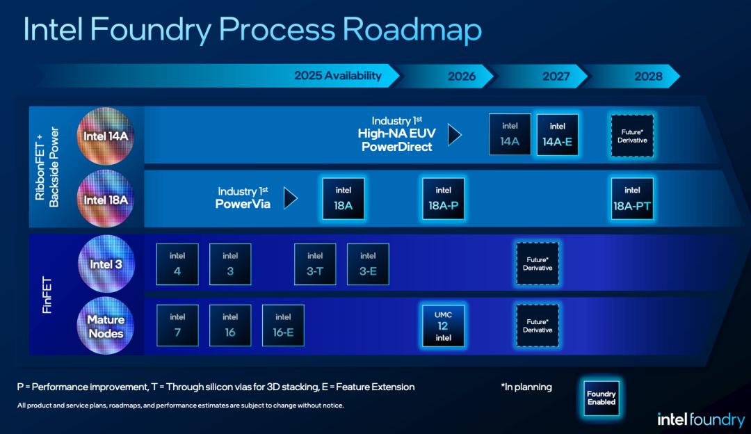
Therefore, Intel's approach can be summarized as: first use High-NA in a small portion of the 18A production layers for "training," then expand its usage in 14A. This path has the highest cost and the greatest risk, but Intel needs to trade technological leadership for time. For TSMC, High-NA is a cost-based choice; for Intel, it is more like a process validation that must be won.
TSMC: Not That It Won't Use It, But That It Doesn't Need It Right Now
TSMC's attitude toward High-NA is clearly more restrained. TSMC holds over 90% of the world's advanced process foundry market share, with giants like Apple and NVIDIA in its supply chain. TSMC's top priority is "helping customers control costs, ensure yield, and deliver stably." Therefore, from the 2nm (N2), A16 to A14 nodes, TSMC has explicitly stated that it does not need to rely on High-NA EUV.
At its Q2 2026 earnings conference, TSMC CEO C.C. Wei openly acknowledged that High-NA is a high-performance tool, but emphasized at the same time that its adoption timeline depends on three conditions: technical capability, maturity, and reasonable cost. Wei also specifically mentioned the half-field issue of High-NA tools. Since High-NA uses a refractive optical system, its single exposure area is only half that of traditional EUV, meaning large-sized chips may require exposure field stitching, which brings challenges to overlay, yield, production efficiency, and design constraints. TSMC will factor all these elements into manufacturing costs.
TSMC's confidence in not adopting High-NA for now lies in the fact that A14 does not depend on it. Without High-NA, what allows TSMC's A14 to achieve a 20% density boost?
TSMC breaks down the resolution benefits that High-NA would have provided across multiple stages — transistors, standard cells, masks, computational lithography, patterning, interconnects, and yield control — extending the 0.33 NA EUV lifespan through a full set of collaborative optimizations. TSMC currently plans to start risk production of A14 in 2027 and achieve mass production in 2028.
Specifically, the primary gain for A14 comes from the transistor itself: A14 uses TSMC's second-generation nanosheet GAA transistor architecture. Compared to N2, A14's latest public targets are: an estimated 10%–15% performance improvement at the same power, or a 25%–30% power reduction at the same performance, along with a nearly 20% increase in logic density.
Another publicly disclosed core technology for A14 is NanoFlex Pro. Through Design-Technology Co-Optimization (DTCO), customers can make more granular trade-offs between performance, power, and area for different functional modules. TSMC Senior Vice President Kevin Zhang once explicitly stated that A14, powered by robust DTCO, has significantly delayed the need for high-NA lithography tools.
The third key point is Low-NA multi-patterning. A14 will still use 0.33 NA EUV as its primary advanced lithography platform, continuing single-exposure for layers that support it, and only adding necessary pattern splitting and multi-patterning for a small number of the densest, most complex critical layers.
Masks are also a critical factor. TSMC is improving the manufacturability of 0.33 NA EUV for extreme patterns through more complex curvilinear masks, higher-resolution multi-electron beam writing, and more precise mask correction. TSMC explicitly disclosed in its annual report that for A14 and more advanced nodes, its mask technology R&D includes: optimizing EUV mask substrate materials, improving the resolution of multi-electron beam mask writing tools, refining mask manufacturing processes, enhancing the critical dimension uniformity of curvilinear patterns, boosting pattern fidelity and overlay accuracy, and using advanced e-beam inspection and repair technologies to reduce mask defects. TSMC is also developing new EUV mask pellicles and mask substrates to improve yield, productivity, and tool utilization efficiency.
TSMC's biggest advantage is precisely that it can afford to wait. It has the largest installed base of NXE tools, mature multi-patterning technology, high capacity utilization, and stable customer demand — there is no need to take on High-NA depreciation prematurely just to prove technological leadership.
This does not mean TSMC is rejecting High-NA. TSMC launched lithography technology development for High-NA scanners back in 2025, but it prefers to wait until the following conditions are met: further improvements in High-NA tool throughput and availability; a mature ecosystem of photoresists, masks, inspection, and metrology; process cost savings from using High-NA exceeding the additional depreciation; sufficient customer orders to amortize tool costs; and the resolution of large-chip half-field stitching issues.
Samsung Is in a Wait-and-See Phase
According to the latest reports from TrendForce and South Korean industry sources, Samsung has completed the installation and deployment of two ASML High-NA EUV tools (including the Twinscan EXE series) at its Hwaseong campus, with total investment exceeding 1 trillion won (approximately $770 million). The first tool arrived in 2025 for R&D and testing, and the second was introduced in the first half of 2026. However, Samsung has not yet formally integrated them into any commercial production lines, and the relevant mass production deployment is generally in a state of suspension and observation.
Industry analysis suggests that Samsung's cautious stance is not due to substandard technology, but rather the severe pressure on its Foundry business's profit and loss statement. A single High-NA tool costs as much as approximately $400 million, nearly twice the price of a traditional Low-NA EUV tool. At a sensitive juncture where the foundry division has been under persistent pressure since 2022 and is striving to break even, forcing these tools into commercial production lines would immediately add massive hardware depreciation, facility operation costs, exclusive photomask expenses, and associated R&D costs to its financial statements, easily dragging the foundry business back into losses.
The practical challenges Samsung faces include: first, the volume of signed customers and order size for advanced nodes (such as 2nm GAA) still lag behind TSMC, and if capacity utilization is insufficient to amortize depreciation, the costs will become unbearable; second, although reports claim Samsung's 2nm trial production yield has made significant progress, High-NA tools cannot automatically solve issues like nanoscale transistor architecture optimization, EDA software design ecosystem maturity, and packaging support; third, caught between Intel's high-profile integration of High-NA into the 18A/14A nodes and TSMC's deliberate, calculation-driven wait-and-see approach, a hasty large-scale production rollout by Samsung would only amplify its fixed-cost risks.
Therefore, Samsung's current more rational strategy is "keeping the tools ready but not putting them into commercial use": retaining the procured High-NA tools in R&D and pilot lines for trial production and process exploration, while strictly controlling the expansion of commercial scale.
In the future, Samsung's most likely breakthrough points remain in the 1.4nm (SF1.4) class logic process, and next-generation vertical channel transistor (VCT) advanced DRAM. Especially in the DRAM field, as the pattern precision of memory cells below 10nm approaches physical limits, the number of mask layers and process complexity of Low-NA multi-patterning rise sharply, so the economic value of High-NA EUV in simplifying workflows via single exposure may become apparent earlier than in logic foundry. However, Samsung has not yet officially announced a clear mass production timeline.
SK Hynix: Extremely Decisive for the Sake of HBM
Unlike logic foundries TSMC and Samsung, which are hesitating over the "half-field" problem and huge costs, memory leader SK Hynix has adopted an extremely decisive path for High-NA EUV.
In September 2025, SK Hynix installed the memory industry's first mass-production High-NA EUV tool at its Icheon M16 fab. Unlike Intel's early pilot-production EXE:5000, the one SK Hynix introduced is ASML's TWINSCAN EXE:5200B — a model truly designed for high-throughput, large-scale mass production (with a wafer throughput of 175+ wafers per hour).
SK Hynix plans to gradually roll out High-NA into its cutting-edge 0a nm-class DRAM, and even future 3D DRAM (vertical structure DRAM) production around 2026-2027.
For logic foundries like TSMC, large chips (such as AI GPUs) face the High-NA "Half-Field cutting and stitching" challenge, which leads to lower exposure efficiency. But the physical properties of memory chips (DRAM) are completely different:
1) Avoiding the multi-patterning nightmare: As DRAM processes evolve to 1b, 1c, and even 0a (sub-10nm) nodes, continuing to use Low-NA EUV would require 3 or even 4 rounds of EUV multi-patterning. This would lead to a sharp increase in mask layers, extremely cumbersome processes, and plummeting yields. High-NA single-exposure can drastically simplify the manufacturing workflow.
2) Meeting the core scaling needs of HBM: HBM's technological iteration imposes extremely strict requirements on the capacitance density and channel line width of underlying DRAM dies. To maintain its absolute dominance in NVIDIA's supply chain, SK Hynix must rely on High-NA to achieve high integration and ultimate performance at smaller feature sizes.
ASML: The Biggest Winner
No matter what plans fabs have in mind, ASML, as the exclusive supplier, remains in an invincible position.
Taking its Q2 2026 financial report as an example: ASML's net sales reached 9.3 billion euros, with a gross margin of 54.0% and a net profit of 2.9 billion euros. Out of 6.6 billion euros in system sales, EUV tools generated approximately 3.8 billion euros in revenue, non-EUV tools around 2.8 billion euros, and only one High-NA system was included in the EUV revenue.
In other words, although High-NA has extremely high strategic value and a high unit price, it is not yet the main driver of ASML's revenue growth.
ASML's real "three engines" are running at full power:
The first is Low-NA EUV.
ASML expects to deliver approximately 65 Low-NA EUV tools in 2026, plans to increase Low-NA EUV capacity by about 30% in 2027, and has already secured a large number of 2028 orders. The underlying reason is simple: 2nm, 3nm, HBM, advanced DRAM, and subsequent nodes still require massive numbers of 0.33 NA EUV tools. Even if some critical layers shift to High-NA, the vast majority of process layers will continue to use the NXE platform.
The second is DUV immersion tools.
ASML plans to increase DUV immersion tool capacity by about 30% in 2027, with current capacity at around 130 units, and is studying a further 30% capacity increase in 2028. This is because not all layers of advanced chips use EUV. A large number of non-critical layers, mature processes, analog chips, power devices, and advanced packaging still require DUV. The emergence of High-NA will not eliminate DUV demand; instead, it may grow in tandem with the overall capacity expansion of fabs.
The third one, which many people might not expect, is installation services and upgrades.
In Q2, ASML's installation and management revenue approached 2.8 billion euros. As the global installed base of EUV and DUV tools expands, maintenance, upgrades, source power enhancement, productivity transformation, and computational lithography services will generate recurring revenue. The value of this segment is that no matter whether customers choose to adopt High-NA early or continue to rely on Low-NA multi-patterning, ASML can generate revenue.
ASML currently expects total net sales in 2026 to be between 43 billion and 45 billion euros, with a gross margin between 54% and 56%.
Final Thoughts
In any case, the competition for High-NA EUV has moved from technical feasibility to economic feasibility.
ASML's High-NA offers 8nm-level resolution, capable of printing feature sizes approximately 1.7 times smaller than 0.33 NA EUV, with a theoretical potential for roughly 2.9x improvement in transistor density, and the possibility of replacing some multi-patterning steps with single exposure. However, tool price, half-field exposure, chip stitching, photoresists, masks, inspection equipment, throughput, and capacity utilization collectively determine whether it is more cost-effective than Low-NA.
The eventual divergence among the four giants is nothing but a reflection of their respective business realities: Intel lacks time, so it is willing to pay a premium for "technological leadership"; Samsung lacks foundry profits, so it dares not recklessly expand fixed depreciation; TSMC has no shortage of technology, so it calmly calculates the optimal ROI; SK Hynix, aiming for absolute moats in HBM, takes the lead in sprinting forward in the memory track; and ASML, capturing orders from all sides, emerges as the biggest winner behind this path divergence.