The Golden Age of Advanced Packaging
In 2026, global packaging and testing manufacturers will collectively launch investment expansion initiatives, marking this year as the "Year of Industry Expansion".
According to data from the industry institution Yole Group, the global advanced packaging market reached approximately $46 billion in 2024, with a compound annual growth rate of 9.5% from 2024 to 2030. By 2030, the market size is expected to exceed $79.4 billion. The explosive demand for computing power has completely restructured the supply-demand relationship in the industrial chain. AI training and inference chips have created rigid demand for ultra-large form-factor packaging, making advanced packaging capacity a core bottleneck restricting the delivery of high-end chips.
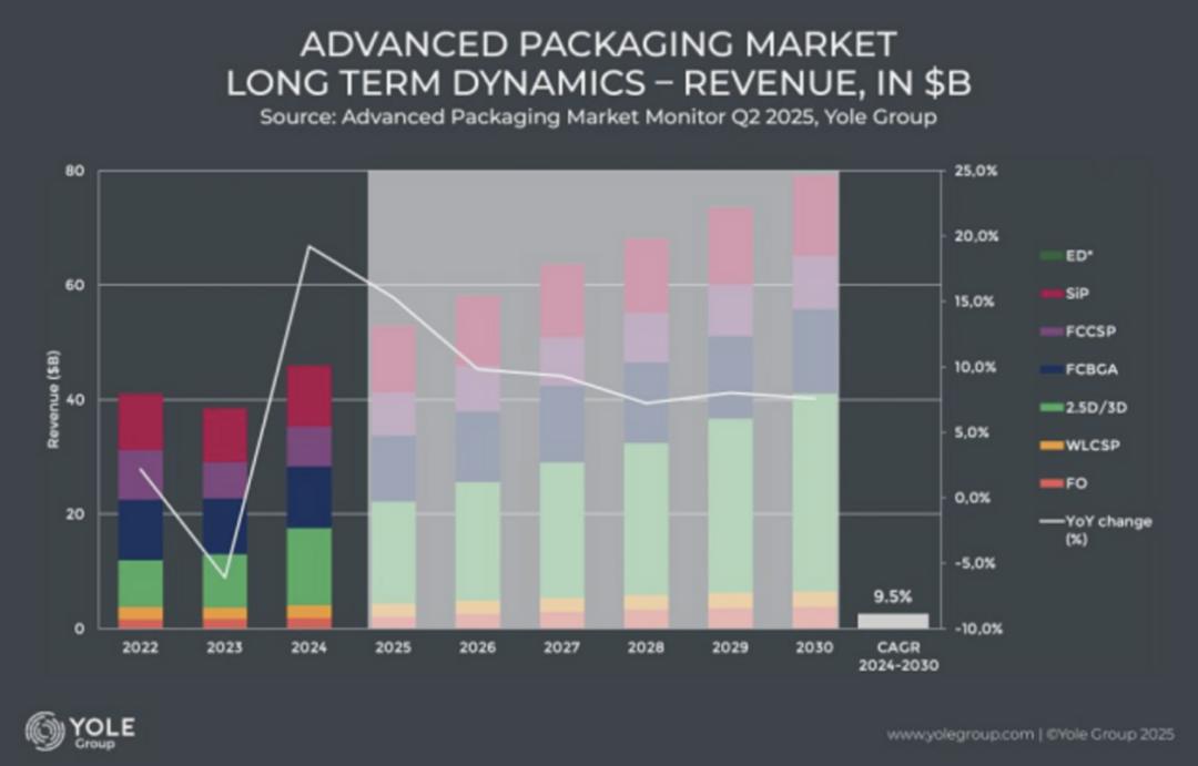
Source: Yole Group
Why 2026?
There is a consensus in the industry that the semiconductor supply and demand follows a cyclical balance pattern. But why are packaging and testing manufacturers collectively launching large-scale capacity expansion in 2026? We can analyze this from three dimensions: demand, technology, and supply chain.
First, from the demand side, the packaging area required for a single high-end AI GPU can reach 2 to 4 times that of a traditional chip. A representative example is NVIDIA's Blackwell series GPUs, which rely on the CoWoS-L process to integrate a single computing die paired with 8 HBM3E memory stacks. As a result, NVIDIA has already secured TSMC's 2026 CoWoS wafer capacity, accounting for more than 50% of TSMC's total annual CoWoS capacity. In addition, companies including AMD's MI300, Google's TPU, Broadcom's AI ASIC, and AWS Trainium have all adopted the CoWoS architecture, which means that the demand for large-size advanced packaging is spreading across the entire product category along the computing power chip track.
At the same time, the development focus of the AI industry is shifting from large model training to massive inference scenarios. A single training chip has a large packaging area but limited overall shipment volume, while the shipment scale of inference chips can reach dozens of times that of training chips, and is highly sensitive to unit packaging costs. This also presents an excellent window for large-scale implementation and verification of panel-level fan-out packaging and low-cost heterogeneous integration solutions.
In addition to the incremental space on the demand side, the iteration of underlying semiconductor technologies is also reshaping the industrial status of the packaging segment. In the post-Moore era, the marginal benefits of planar transistor scaling continue to narrow, and the construction and R&D costs of advanced wafer fabs at 3nm and below are rising exponentially. The main line of industrial development is gradually shifting to Chiplet die disaggregation and heterogeneous integration solutions. This combined solution breaks down a single large chip into chiplets adapted to different processes, and then relies on advanced packaging to complete high-density interconnection, directly upgrading packaging from a traditional back-end assembly process to a core manufacturing link that determines the computing power, bandwidth, and yield of chips.
Finally, from the supply chain dimension, the global geopolitical supply chain is being restructured, and regions such as the United States and Southeast Asia are accelerating the establishment of local supporting systems for chip manufacturing and packaging and testing. Enterprises need to disperse their production capacity across multiple regions to reduce supply chain risks. Under the combination of multiple factors, global packaging and testing manufacturers will simultaneously launch capacity expansion in 2026.
Overseas Giants Are Expanding Aggressively
TSMC is the absolute leader in the AI computing power chip CoWoS packaging track. According to overall calculations by top brokerages such as Morgan Stanley and Mizuho, TSMC's global CoWoS capacity will account for about 70% of the total market share in 2026. Facing the continuously rising demand for computing power packaging orders, TSMC disclosed at its corporate briefing that the company's total capital expenditure in 2026 is locked at $52-56 billion, with 10% to 20% of the resources allocated to advanced packaging processes such as CoWoS.
In terms of capacity expansion, TSMC is promoting CoWoS expansion through a dual-track model of renovating 8-inch old fabs and building new dedicated plants. Among them, the two core bases of Chiayi AP7 and Southern Science Park AP8 continue to launch dedicated packaging production lines with a clear capacity ramp-up pace. The capacity target for the fourth quarter of 2026 is raised to 130,000-140,000 wafers, and the monthly capacity is expected to reach 190,000-200,000 wafers by the end of 2027.
In terms of overseas layout, TSMC has made multiple rounds of additional investments in its Arizona project in the United States, with a total planned cumulative investment of $165 billion. The latest expansion plan for this project includes 8 wafer fabs and 4 advanced packaging facilities. The market generally estimates that the first local packaging production line will be put into mass production around 2028. Meanwhile, TSMC is also developing the next-generation panel-level CoPoS packaging technology. Its subsidiary, Coretronic, has completed a CoPoS pilot line in the Longtan plant, and NVIDIA's next-generation Feynman architecture GPUs are expected to be among the first products to be implemented.
However, TSMC is not the only enterprise accelerating the expansion of advanced packaging capacity driven by the demand for high-end CoWoS. A large number of OSAT manufacturers are also increasing their efforts in layout.
According to industry insiders, ASE is currently in the largest factory expansion cycle in the company's history. CEO Wu Tianyu revealed that in 2026, six new packaging and testing plants of ASE around the world will start construction simultaneously, with the largest expansion intensity over the years. Multiple brokerages predict that ASE's monthly CoWoS capacity will ramp up from 20,000 wafers at the end of 2026 to 40,000-45,000 wafers by the end of 2027; institutions also estimate that its LEAP advanced packaging platform is expected to generate revenue exceeding $3.5 billion in 2026.
In terms of physical investment, ASE plans to invest more than NT$108.3 billion (about $3.4 billion) in the Kaohsiung Renwu base, NT$35.2 billion (about $1.09 billion) in the Nanzih K19A park supporting investment, and spend NT$14.85 billion (about $480 million) to acquire Innolux's Southern Science Park Fab5 plant to expand its advanced production lines.
In terms of technology layout, Wu Tianyu revealed that ASE's CPO (co-packaged optics) business will start small-scale trial production in 2026. This solution integrates optical engines and ASIC chips into the same substrate through advanced packaging, replacing traditional discrete pluggable optical modules. It is the core route for AI data centers to increase interconnection bandwidth. ASE taking the lead in implementing CPO trial production also represents that leading OSATs are expanding their technical boundaries from traditional pure packaging and testing to optoelectronic integrated integration.
Amkor, another giant in the OSAT camp, is also actively expanding, with its core global expansion base located in Arizona, USA. In June 2026, Amkor signed a ten-year long-term cooperation agreement with TSMC, under which TSMC will purchase local CoWoS packaging and testing capacity from Amkor to support wafer manufacturing. In this regard, Amkor CEO Kevin Engel commented that this cooperation is a key layout for building a complete domestic supply chain of "advanced wafer manufacturing - packaging and testing" in the United States.
In terms of capital allocation, Amkor's annual capital expenditure is about $2.5-3 billion, of which 65%-70% is used for infrastructure expansion of global plants, and the remaining 30%-35% is used to purchase 2.5D and HDFO high-density fan-out advanced packaging equipment, with the equipment procurement budget increasing by 40% year-on-year. In terms of capacity layout, Amkor has built an Intel EMIB embedded bridge packaging production line at the Songdo K5 plant in South Korea and is gradually ramping up capacity, while continuing to expand its Vietnam plant to meet the order demand for FOWLP fan-out and heterogeneous integration.
In addition to computing power chips, the strong demand for HBM memory chips is also driving the advanced packaging and testing capabilities of memory giants. Both Samsung and SK Hynix have deployed cross-border packaging and testing bases to strengthen the memory packaging and testing supply chain.
Samsung plans to build a packaging and testing base in Thai Nguyen Province, Vietnam. The total phased investment of the project is planned at $4 billion, with the first phase investing $2 billion. The plant will initially focus on traditional memory chip testing services, and expand HBM packaging capacity in the long run. SK Hynix is building the P&T7 integrated plant in Cheongju, South Korea, with a total investment of 19 trillion won (about $12.9 billion). The plant covers the entire process of wafer testing and HBM advanced packaging. Combined with the existing mature production lines in Icheon, Gyeonggi Province, and the $3.87 billion HBM dedicated packaging base in West Lafayette, Indiana, USA, SK Hynix has established three global advanced packaging centers in Icheon, Cheongju, and West Lafayette, USA.
Domestic Leaders Are Accelerating Investment
Against the tide of simultaneous capacity expansion by overseas manufacturers, leading domestic packaging and testing enterprises have also intensively announced large-scale expansion plans in the first half of 2026. All new projects are focused on high-end cutting-edge processes such as HBM, 2.5D, Chiplet, and CPO. The local packaging and testing industry has officially moved from the stage of low- and mid-end domestic substitution to a new cycle of independent layout of high-end advanced packaging and testing technologies.
JCET plans to invest a total of 7.8 billion yuan to build a high-end packaging and testing base in Lingang, Shanghai. The project is divided into two phases of construction. The first phase of the plant is expected to be put into operation in the second half of 2028, focusing on four core processes: 2.5D/3D stacking, HBM3E multi-layer memory stacking, Chiplet heterogeneous integration, and CPO optoelectronic co-packaging. As the only local packaging and testing manufacturer in mainland China that has achieved large-scale mass production of HBM3E multi-layer memory stacking, JCET's customer resources cover leading domestic and overseas enterprises such as NVIDIA, HiSilicon, and SK Hynix.
Ningbo Yongsi Electronics has also launched a tens-of-billion-level investment. The total investment in the third phase of the Ningbo Yuyao microelectronics high-end IC packaging and testing project is 10.3 billion yuan, with an overall construction period of up to 8 years. The project comprehensively deploys a full range of processes such as BUMP wafer bumping, 2.5D heterogeneous packaging, FC flip-chip packaging, and wire bonding, to fill the gap in domestic wafer-level packaging capacity.
Tongfu Microelectronics has implemented a private placement financing plan of 4.22 billion yuan, and disclosed that the total capital expenditure in 2026 will reach 9.1 billion yuan, with capacity investment focusing on the advanced packaging and testing tracks of computing power chips and high-end memory.
Using its holding subsidiary Huatian Nanjing as the platform, Huatian Technology has raised 3 billion yuan to build a dedicated advanced memory packaging and testing production line, specializing in the packaging and testing of high-end memory chips such as DDR5 and HBM, and continuously consolidating the supporting capabilities of domestic memory chips.
The four leading local packaging and testing enterprises are simultaneously increasing their high-end capacity, and this move has dual significance for industrial profitability and supply chain security. Against the background of the decentralization of the geopolitical supply chain, the domestic advanced packaging supply capacity will be rapidly supplemented, gradually weakening the monopoly advantage of overseas manufacturers in the field of high-end computing power packaging. In the short term, new domestic capacity will prioritize undertaking orders for domestic computing power and memory chips to complete the closed-loop supporting of the local industrial chain. In the medium and long term, with the continuous iteration of the yield of HBM, 2.5D, and CPO processes, local packaging and testing manufacturers will have the opportunity to enter the supply chain of global overseas customers, truly realizing the leap from "capacity replenishment" to "double breakthroughs in technology and customers".
Hidden Variables Under Expansion
This global packaging and testing expansion arms race triggered by AI computing power demand is continuously promoting the shift of the semiconductor industrial chain's value focus from front-end wafer manufacturing to mid-end advanced packaging. Global packaging and testing manufacturers have different expansion logics, with significant differences in technical routes, customer structures, and capacity layouts. This means that advanced packaging has not yet entered a stable competitive landscape. Under the short-term high prosperity, there are multiple variables and constraints in the long-term development of the industry.
From the perspective of capital investment, this round of expansion is a high-threshold and heavy-asset game. The investment scale for a monthly capacity of 10,000 wafers in advanced packaging is close to that of a 14nm wafer fab, and the investment in a single high-end production line often reaches the tens of billions level. Global manufacturers rely on large capital expenditures and private placement financing to promote plant construction, which continuously increases the cash flow pressure on enterprises in the long run. The short-term shortage of AI computing power supports the high gross profit margin of high-end packaging, but after a large number of new capacities are concentrated and launched in 2027, the competition in industry foundry quotations may intensify. Only leading enterprises that are tied to leading computing power and memory customers and master high-end processes can maintain profitability resilience.
At the same time, the ceiling of upstream equipment and material supply objectively restricts the implementation pace of this round of expansion. The supply of high-precision bonding and wafer metrology equipment for advanced packaging is tight, with delivery cycles generally extended to more than one year, and the capacity of ultra-large-size high-end substrates adapted to CoWoS and HBM is also in short supply. Domestic manufacturers are highly dependent on foreign countries for high-end equipment and special materials, and overseas export controls continue to exist. The release pace of local advanced packaging capacity has long been constrained by the shortcomings of upstream supporting facilities.
When the global giants simultaneously launch large-scale advanced packaging capacity, the advanced packaging market is likely to usher in a key inflection point in the supply-demand pattern in 2028. Whether the expansion dividends brought by the short-term shortage of computing power can continue depends on multiple variables such as the long-term demand growth rate of the AI industry, the mass production implementation progress of new technologies, and the changes in the global geopolitical supply chain. By then, whether the packaging and testing market will maintain a supply-demand balance or face partial overcapacity, we will wait and see.
This article is from the WeChat public account "Semiconductor Industry Observation" (ID: icbank), author: Xia Xue, authorized by 36Kr for release.