Musk's scalpel, lithography machine and chip factory
Elon Musk is set to make a radical overhaul of EUV lithography machines.
To break the physical dependence of traditional extreme ultraviolet lithography on independent light sources for individual machines, Musk has directly set his sights on industrial-grade free-electron lasers (FEL).
On August 6 local time in the United States, the official SpaceX account released a night render video of the Terafab giant chip fab, and the huge circular synchrotron ring structure in the center of the frame quickly sparked widespread heated discussion.
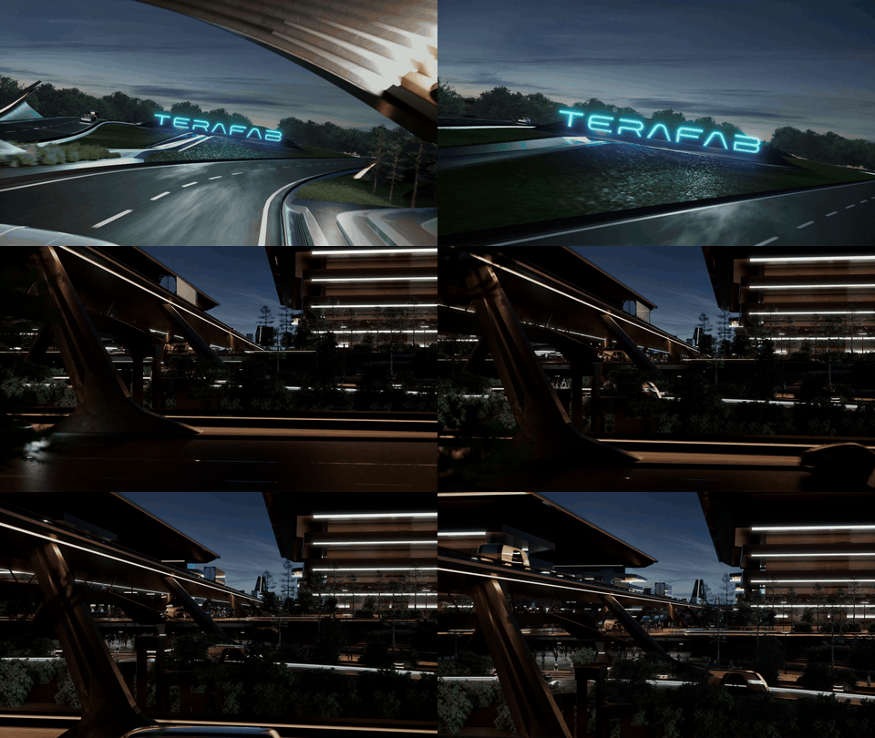
Terafab render video officially released by SpaceX
Extropic founder and former Google quantum computing engineer @beffjezos speculates that Musk may plan to build a free-electron laser-based EUV lithography light source for this wafer fab.
A day later, Musk personally replied: "FEL FTW". (Note: Free Electron Laser, For The Win).
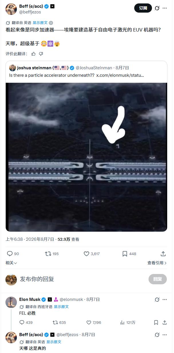
The implementation of the FEL light source solution directly targets ASML's monopoly position in the EUV lithography field, behind which lies Musk's blueprint for a "chip manufacturing factory".
The Terafab project jointly invested by SpaceX and Tesla is advancing at the site of a decommissioned coal-fired power plant in Grimes County, Texas. The first phase has an investment of 16.8 billion US dollars, with a planned manufacturing space of over 100 million square feet (approximately 9.29 million square meters).
The FEL light source is precisely one of the core technical bets of this super factory.
01
Why Can It Challenge ASML?
Chip giants such as TSMC, Samsung, and Intel rely extremely heavily on ASML's EUV lithography machines when manufacturing chips with advanced global process nodes.
The light source of ASML's EUV lithography machines comes from an in-house high-power carbon dioxide laser, which strikes tiny molten tin droplets at a frequency of about 50,000 times per second. Each tin droplet is hit twice in a row, vaporized into extremely high-temperature plasma (LPP) that radiates EUV light, which is then collected by a curved mirror and directed to the wafer.
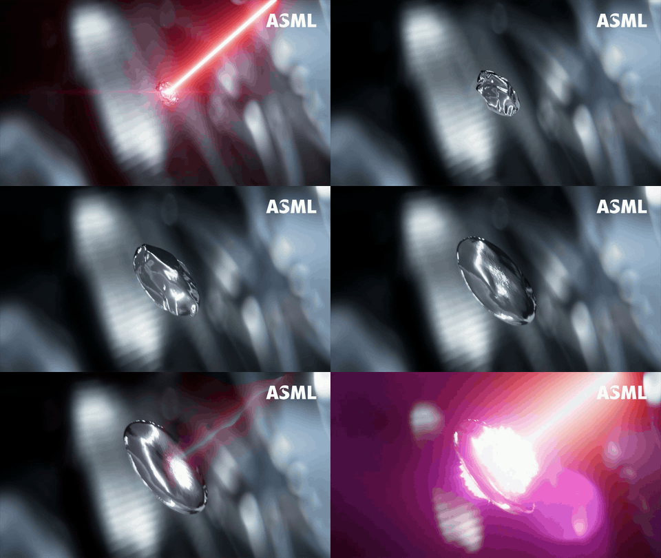
Principle of ASML EUV light generation: The laser strikes tiny molten tin droplets. Source: X Platform
This solution underpins the current EUV chip era, but it also faces insurmountable physical limitations.
First of all, the energy efficiency is extremely low, and most of the electric power is converted into waste heat during the process of heating the tin droplets. Secondly, tin will leave debris contamination after vaporization and erode expensive precision mirrors, greatly increasing the equipment's maintenance downtime. Finally, as the demand for exposure power continues to rise, the complexity of the distributed standalone system is approaching its physical limit.
In contrast, the working principle of free-electron lasers (FEL) is completely different.
The FEL solution planned by Terafab uses a particle accelerator to accelerate electron beams to directly generate light through radiation, adopting a centralized central power station model where one accelerator ring distributes the light source to dozens of lithography machines.
Renowned investor and Hallid.ai founder @indigo explains that FEL first strips free electrons from atoms, accelerates them to near the speed of light via a particle accelerator, and then passes the high-speed electron beam through a wiggler composed of alternating magnets. The magnetic field forces the electrons to swing at high speed along a wavy path and radiate electromagnetic waves. When a large number of coherent electrons move together, the emitted light will self-amplify, forming an intense and highly focused beam.
By adjusting the electron energy and the spacing between magnets, FEL can precisely tune the output wavelength, including the 13.5-nanometer light source required for chip manufacturing.
The advantage of the FEL solution lies in its clean light source with zero tin contamination and extremely low loss of optical lenses, which can not only greatly reduce downtime maintenance, but according to data from Japan's KEK laboratory, under the same EUV power output, its energy consumption can be reduced to 1/4 to 1/5 of that of traditional systems.
In addition, FEL can precisely tune the output wavelength, including the 13.5-nanometer light source required for chip manufacturing. Theoretically, it can be seamlessly extended to 6.x nanometers or even shorter wavelengths in the future.
indigo sums up this solution as "redesigning lithography with first principles".
This change at the architectural level is the most fundamental. It turns light into a public infrastructure just like water, electricity and gas. The circular accelerator in the Terafab render is exactly the central hub that centrally generates photons and distributes them to the exposure equipment across the factory on demand.
Around 2015, ASML also conducted in-depth evaluations of accelerator light sources, but ultimately chose the lower-risk, more easily modular plasma radiation light source route due to the huge size of accelerators, the extremely high reliability requirements for industrial-grade continuous operation, and the huge initial investment.
Startups including xLight are also advancing the commercialization of centralized FEL light sources, targeting to deliver prototypes in 2028, but no company has yet successfully delivered an industrial-grade system.
China is also exploring similar "lithography fab" solutions, where EUV beams are generated by a light source factory and transmitted to dozens of adjacent lithography exposure stations for simultaneous operation.
The reason why Terafab dares to bet on FEL essentially stems from its huge production capacity demand.
At the super-scale planned to produce 1 terawatt of computing power per year, the high operation and maintenance costs and huge energy consumption of the distributed tin plasma solution will be unbearable, while FEL's originally high initial investment will be greatly diluted, thus turning from a high-risk alternative into an economically viable option.
02
Decommissioned Power Plant Gets a New Lease of Life
The main site of Terafab is located in Gibbons Creek, Grimes County, Texas, at the former site of a coal-fired power plant decommissioned in 2019. The Gibbons Creek Reservoir near the old power plant has been used for cooling coal-fired units for decades, and what Musk's team values is exactly its unique legacy of infrastructure.
Terafab plans to use the reservoir to collect rainwater and surface water for on-site recycling, and cooperate with supporting on-site wastewater treatment facilities to realize closed-loop operation of water resources, completely avoiding pumping local groundwater.
In terms of energy supply, Terafab adopts an independent solution completely disconnected from Texas' public power grid. It builds an independent on-site natural gas power plant to generate power on its own, which can not only completely avoid the impact of external grid fluctuations on the production continuity of the wafer fab, but also eliminate the impact on local residents' power load.
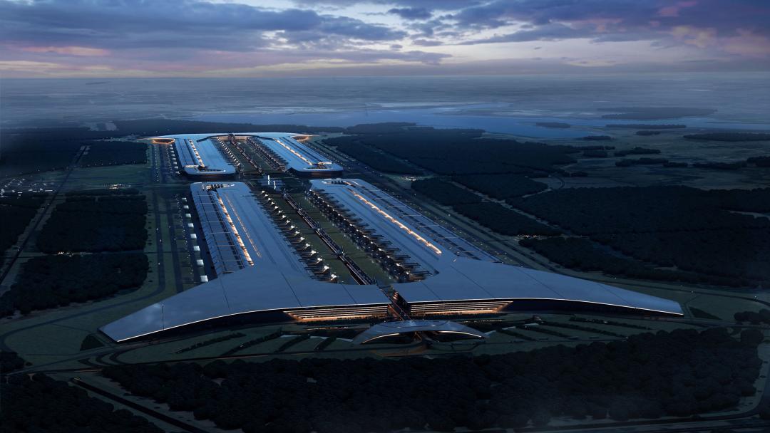
Source: SpaceX official website
The scale of the entire project has refreshed the record for industrial buildings.
The size comparison diagram shared by Musk shows that after completion, Terafab will be 50 times the area of the Pentagon, with its main building about 2.5 miles long. It consists of four giant buildings that integrate the whole process of logic chip manufacturing, memory chip manufacturing, advanced packaging and testing under one roof, breaking the traditional semiconductor industry pattern where links are scattered across multiple suppliers.
According to SpaceX's filing documents, the overall construction window of the project is as long as 11 years (from 2026 to 2037), which will be advanced in multiple phases, and mass production is expected to start in 2029.
In terms of capital investment, the first phase of 16.8 billion US dollars is jointly funded by SpaceX and Tesla, and the long-term total investment plan may reach as high as 119 billion US dollars. In addition, the Texas government has provided a grant of about 30 million US dollars through the Texas Enterprise Fund (TEF).
In terms of local cooperation and fiscal and tax arrangements, the first phase of the project will employ at least 3,000 people, 60% to 80% of whom are expected to be recruited from Grimes County and adjacent Brazos County.
The tax agreement shows that the project enjoys a tax reduction of about 78%. In return, SpaceX and Tesla promise to pay Grimes County a fixed 20 million US dollars per year for 35 years, with a total amount of about 710 million US dollars. The first payment of 10 million US dollars has been remitted in advance, which is equivalent to about 40% of the county's annual property tax revenue.
It is worth noting that before the construction of the giant campus in Grimes County starts, a key pre-requisite "seed project" has already broken ground in the north campus of Tesla's Texas Gigafactory.
This is a research pilot production wafer fab with an investment of about 3 billion US dollars, built around Intel's latest process technology and expected to be completed next year. It will serve as the technical verification line for Terafab, allowing the testing and verification of chip process recipes in advance without waiting for the full completion of the giant campus.
03
Musk is Set to Compete Against Three Industry Giants Simultaneously
The design logic of Terafab is to integrate the functions of TSMC, Micron and NVIDIA under the same roof.
In the traditional AI chip production chain, design, logic circuit manufacturing, memory chip production, packaging and mask making are often scattered across different companies and regions. A single process modification may require months of repeated confirmation among multiple suppliers. Terafab highly centralizes these links, allowing engineers from design, manufacturing, memory, packaging and testing to collaborate in real time within the same facility.
This vertical integration model has been practiced by Tesla on the car production line of its Texas Gigafactory before, where casting, painting and final assembly are closely adjacent. Now the only difference is that the integrated object has been changed from cars to silicon wafers.
The product line precisely corresponds to three business needs and flows to three end application fields.
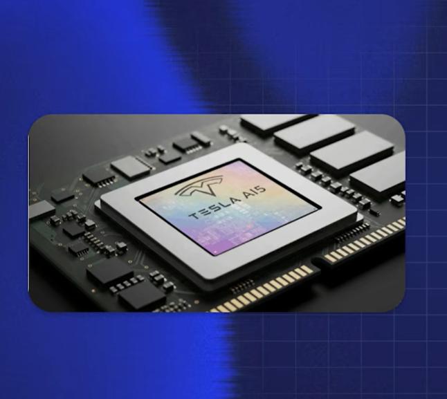
The first is Tesla's hardware: the AI5 chip is specially designed for Tesla Full Self-Driving (FSD) and Optimus humanoid robots, and it is an inference chip with extremely low power consumption. Its design has been taped out this spring, silicon samples are expected to be produced later this year, and mass production is scheduled for 2027.
Source: Brighter with Herbert video
Musk once described the urgency of getting the AI5 right as "a matter of life and death".
The follow-up chip AI6 for the mass production of Optimus and heavier AI workloads is targeted to tape out in December this year, with mass production planned for 2027, and Samsung signed a 16.5 billion US dollar supply agreement for it last summer.
The AI5 and AI6 chips will be fully deployed in Cybercab autonomous vehicles and Optimus robots in the future.
The second is ground data centers: SpaceX, after integrating xAI, currently operates about 1.4 GW of computing power, which is expected to reach 2 GW by the end of the year and rise to about 10 GW by 2027. Chips produced by Terafab will provide independent hardware support for it, gradually reducing its dependence on external general-purpose GPU foundry services.
Source: Brighter with Herbert video
The third is space computing and the StarMind AI satellite. SpaceX is cooperating with NVIDIA to design data center-level space computing payloads for the StarMind AI 1 satellite, combining D3 ruggedized chips and NVIDIA hardware, with the first launch planned for 2027.
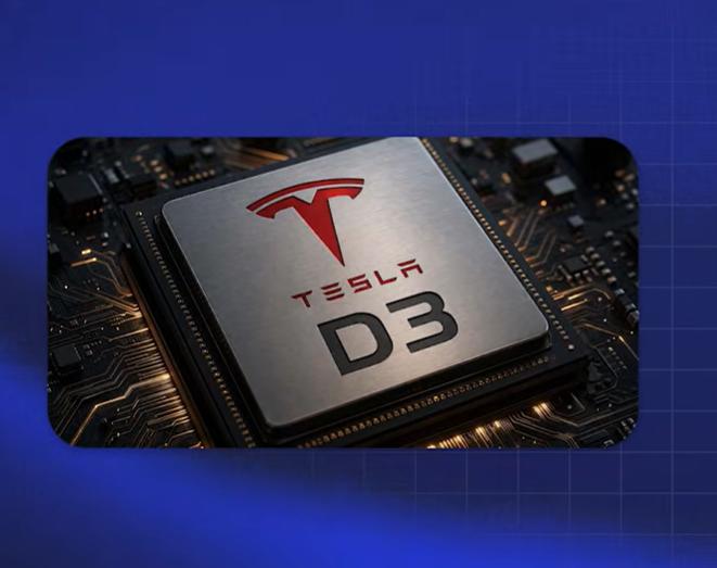
The D3 chip is a space chip ruggedized against radiation and extreme temperature changes, used for SpaceX's space data centers.
Regarding capacity allocation, Musk made a "very rough guess": about 25% of Terafab's AI computing output in the future will be allocated to Tesla hardware such as Optimus, and about 75% will be used in the space AI field and spacecraft.
The necessity and urgency of Terafab precisely stem from Samsung's "lagging behind".
Data shows that part of the reason why the mass production of AI5 was postponed to 2027 is that Samsung encountered delays in its 2-nanometer process this year, and relying on external foundries means inheriting the schedule risks of the other party.
Production capacity is the deeper bottleneck. Tesla aims to produce millions of Optimus robots and Cybercabs every year, and each device requires chips. Musk judges that no foundry on Earth has enough spare production capacity to sell.
04
The Gap Between Ambition and Reality
Terafab's plan shows extremely strong strategic forward-lookingness, but we must also clearly recognize the huge engineering challenges it faces.
In terms of implementation, the first-phase capital of 16.8 billion US dollars, the construction of the Texas research wafer fab, the signing of the tax agreement and the arrival of the remitted funds have all been implemented. Intel's technical support and Samsung's short-term foundry guarantee also ensure the advancement of the near-term roadmap.
However, in terms of the yet-to-be-verified dimensions, the challenges remain severe. First is the uncertainty of FEL industrialization: the stability of particle accelerators in a laboratory environment and in an all-weather high-intensity industrial production environment are two completely different concepts. Any tiny fluctuation in the beam will directly affect the wafer yield, which is exactly why the semiconductor industry did not choose this route in the past.
Secondly, the operation of wafer fabs has an extremely high threshold, and the yield improvement of advanced process nodes relies on decades of accumulated micro process details. Even traditional giants such as Intel have experienced long twists and turns in advancing advanced processes. It remains to be seen whether a company that has never operated a wafer fab before can cross this technical gap in a short period of time.
Finally, there is the