Will SbS, which is a huge headache for other mobile phone manufacturers, become Samsung's trump card?
Recently, there are leaks suggesting that Samsung may adopt the 2nm SF2P process and SbS packaging architecture to develop its next-generation flagship self-developed SoC Exynos 2700. It is claimed that this new chip will push the peak main frequency to 4.20GHz, delivering a significant performance improvement over the previous-generation 3.9GHz Exynos 2600.
Regarding this news, many netizens have targeted their doubts at the yield rate and actual performance of the SF2P process. After all, Samsung's previous generations of self-developed flagship main control chips were constrained by the manufacturing process and performed poorly in energy efficiency, so it is natural for the outside world to raise doubts and even hold a "watching the fun" mentality. But from our perspective at 3eLife, SF2P is "not that important". The brand-new SbS packaging architecture is the "killer feature" that may allow Samsung to outperform competitors and reshape the pattern of the high-end chip market.
What is SbS? It subverts the existing form of chips
Many people may be very unfamiliar with SbS packaging. To understand its value, it is first necessary to clarify its technical principle.
The full name of SbS is "Side-by-Side Packaging", which is a new-generation chip integration solution developed by Samsung based on FOWLP (Fan-Out Wafer Level Packaging). Its essence is to break the traditional vertical stacking layout of SoC and memory chips, and realize horizontal integrated packaging of chips.
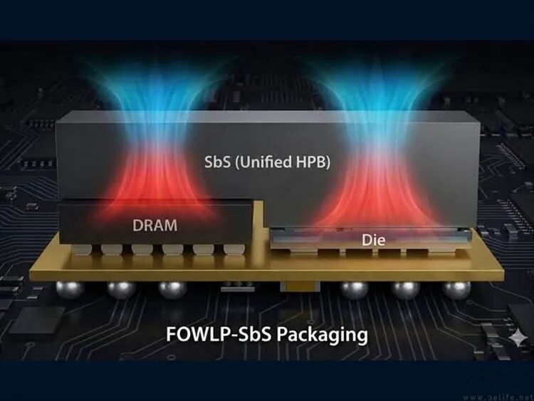
Under this architecture, the SoC main control and DRAM memory are no longer stacked vertically, but arranged side by side on the same plane, and then covered with an HPB heat dissipation module. This not only supports faster and more stable high-frequency memory, but also solves the heat accumulation problem caused by the traditional POP packaging that "covers a quilt" over the SoC with memory.
Some people may think that in POP packaging, the memory is directly stacked on the SoC, so the distance between the two chips is shorter and the transmission delay is lower, right? In fact, that is not the case. Because inside the SoC, the memory controller is usually located at the edge of the chip. If POP packaging is adopted, the memory signal actually follows a routing path that "goes down first and then goes up".
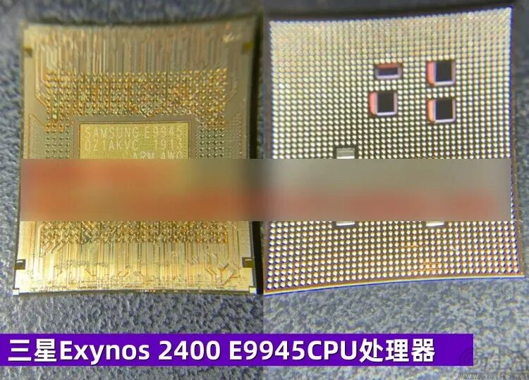
The memory mounting position of POP packaged SoC actually routes up from the bottom
That is to say, inside the SoC, the memory signal needs to first route downward from the controller at the edge of the SoC, pass through the bottom of the package, then detour horizontally, and finally turn back upward to connect to the memory particles on the top layer. The whole process involves a large number of invalid routing paths, vias and corners. The signal transmission path is long and tortuous, which not only greatly increases the wiring distance, but also generates additional signal loss and transmission delay. Moreover, under the high-frequency working condition of the memory, the problems of interference and delay will be further amplified.
In contrast, SbS packaging can arrange the memory particles "exactly" at the edge of the SoC, the position closest to the memory controller. Since there is no need for detour routing and it adopts direct "point-to-point" connection, the data transmission distance is greatly shortened at the physical level.
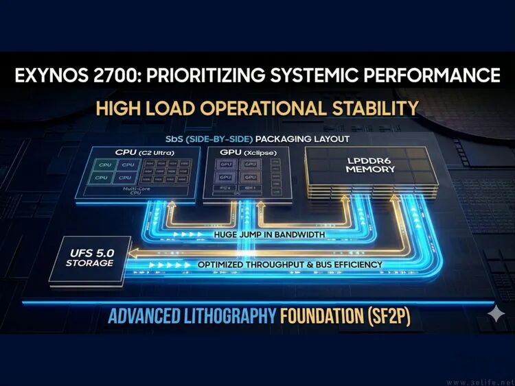
For this reason, according to the currently exposed data, the memory bandwidth of Exynos 2700 can achieve a significant increase of 30% to 40%, bringing faster application startup speed, smoother multi-task background switching, and stable performance in high-load scenarios such as high-frame-rate games and video shooting. In addition, the horizontal layout can also optimize the overall thickness of the chip, reserve more redundancy for the thinning of the device body and the stacking of internal space, and balance performance, heat dissipation and device design.
Why is Samsung the first to try it? It is not just driven by performance pressure
Then why does Samsung take the lead in trying SbS packaging? Many people may think of Samsung's previous launch of HPB packaging, and believe that this is a remedy for Samsung's shortcomings in process technology, a helpless compromise of "poor process, make up for it with packaging". But things may be far more complicated than that. Samsung taking the lead in implementing SbS packaging is actually more like an action to accurately lay out industry advantages and build technical barriers.

First of all, it should be noted that the current mainstream PoP packaging is essentially a split solution with separated SoC and memory. The SoC main control and memory are two completely independent chips, and chip manufacturers such as Samsung only ship bare dies. After terminal manufacturers purchase them, they will complete the stacking assembly, welding and packaging processes of SoC and memory particles on their own production lines. In short, under the PoP mode, the initiative of the main control chip, memory selection and assembly packaging is completely in the hands of terminal manufacturers.
In contrast, SbS is an integrated pre-packaging solution that completely changes the division of labor in the supply chain. Before shipping the main control chip, Samsung will complete the integrated side-by-side packaging, calibration and adaptation of the SoC and the memory of corresponding specifications. What is directly shipped is the integrated "SoC + memory" module, which terminal manufacturers can directly use for complete machine assembly after receiving.

So what does this mean? First of all, as a top global semiconductor giant, the process precision of Samsung's professional packaging production line is far beyond the reach of the SMT assembly production lines of ordinary mobile phone manufacturers. SbS integrated packaging avoids process errors, cold joints, desoldering and other problems that may occur during secondary welding by terminal manufacturers from the source, and completely eliminates the problems of crashes and restarts caused by memory desoldering after long-term use of mobile phones.
More importantly, the most easily overlooked core point is that the SbS packaging method, where the SoC is already bound to the memory before the chip leaves the factory, completely changes the product iteration and inventory strategy of the mobile phone industry, bringing challenges to the vast majority of terminal manufacturers.
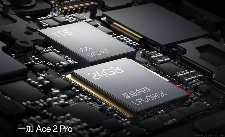
Under the PoP packaging mode, if a terminal manufacturer plans to equip 12GB of memory in the early stage and purchases the corresponding SoC in advance, but the price of memory drops sharply on the eve of the new phone's launch, the manufacturer can completely adjust the plan temporarily, re-purchase 16GB memory with higher cost performance, and complete welding and assembly by itself, so as to quickly upgrade the configuration and improve product competitiveness.
However, under the SbS packaging mode, such space for flexible adjustment disappears completely. Since the 12GB memory has been packaged with the SoC main control at the factory, it cannot be disassembled and replaced separately. If the market situation changes and the product configuration needs to be upgraded, the terminal manufacturer will not be able to replace the memory particles alone, and can only abandon all the original inventory of SbS packaged chips and re-purchase new modules equipped with 16GB memory. This will undoubtedly bring extremely high inventory loss and sunk cost, thereby compressing the profit margin of the product.
Taking the lead in trying advanced packaging, Samsung is targeting the future of the industry
For this reason, the popularization of SbS packaging is bound to bring disruptive challenges to the vast majority of mobile phone manufacturers that lack self-developed chips and memory production capacity. It will force them to accurately predict the future memory market situation from the very beginning of product project approval, with almost no room for trial and error.
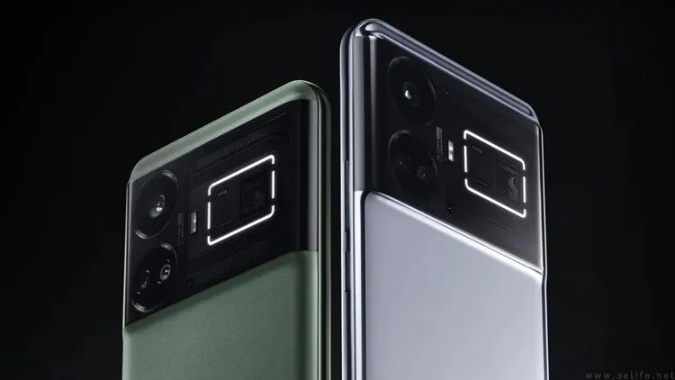
At the same time, in order to avoid inventory risks, the sales cycle of a single model may be further shortened, and the pace of product iteration will continue to accelerate. In addition, terminal manufacturers are likely to adopt a differentiated strategy, applying the high-bandwidth, low-heat, high-cost SbS packaging only to ultra-flagship models, while ordinary high-end models will still use the PoP packaging solution with mature technology, flexible adjustment, lower cost, but slightly weaker heat dissipation and performance.
However, this rule, which is quite strict for other manufacturers, puts no pressure on Samsung itself, and may even be transformed into an exclusive market advantage. After all, looking at the global mobile phone industry chain, Samsung is one of the very few enterprises that have independent production capacity of memory particles, self-development capability of high-end chips, and top wafer packaging production lines, and have realized full-link independent control of "memory production - chip design - packaging and testing".

This advantage of the entire industrial chain gives Samsung unparalleled flexibility that other terminal manufacturers cannot match. They can adjust the memory specifications and capacity ratio of SbS packaged chips in real time according to the new phone planning and market price fluctuations, accurately control inventory risks, and do not need to bear high sunk costs. While other manufacturers are constrained by the shortcomings of the supply chain and can only passively adapt to the market rules, Samsung can take the lead in the pace of product iteration and maximize the value of SbS.
Therefore, SbS packaging is not so much a blind "first to try" technical attempt by Samsung, but rather a strategic layout based on its own full industrial chain advantages and accurately positioning in the high-end market. Excessive focus on the yield controversy of the SF2P process is actually putting the cart before the horse. After all, process iteration is only a basic upgrade, and SbS packaging may be Samsung's hidden card to break through the triple bottlenecks of performance, heat dissipation and supply chain.
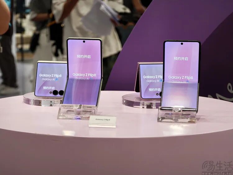
As the performance of flagship mobile phones continues to intensify in involution, the drawbacks of traditional PoP packaging will continue to expand, and the replacement trend of SbS packaging architecture is already clear. In the future, as PoP packaging is gradually phased out, with the technical barriers and industrial chain advantages built by SbS packaging, Samsung is expected to completely get rid of the past shortcomings in the reputation of its self-developed chips. Its demand potential in the high-end chip market, advantages in process yield, and flexibility in product iteration will be fully released, and it may even achieve a counterattack.
This article is from the WeChat Official Account "3eLife" (ID: IT-3eLife), written by San Yijun, and published by 36Kr with authorization.