Are optical computing chips on the verge of mass production?
For more than half a century, Moore's Law has been the underlying logic driving global computing power iteration: the manufacturing process keeps shrinking, the number of transistors keeps increasing, and the computing performance of chips keeps improving. However, this development model is soon reaching its limit.
Nowadays, the parameter scale of large models is expanding at an almost uncontrollable speed, the growth cycle of computing demand is constantly being compressed, but the physical ceiling of electronic chips has become clearly visible. The power consumption wall, memory wall and bandwidth wall are three major bottlenecks that strictly restrict the evolution pace of traditional GPUs. The higher-end the computing chip, the higher its power consumption, the more difficult heat dissipation becomes, and the more severe the invalid loss caused by data transmission.
Simply put: the path of increasing computing power by stacking transistors is no longer feasible. The industry is in urgent need of a brand-new solution, and using light instead of electricity for computing has become the most disruptive and most promising answer at present.
At the 2026 WAIC that concluded not long ago, the optical computing track went all out, with three leading domestic enterprises showing their core technologies intensively:
Optical Core Technology announced that it has successfully taped out a photonic in-memory computing chip with a 256*256 matrix scale for the first time. This chip is currently the optical computing chip with the highest computing power density and highest computing precision in the world, and is mainly oriented to high-computing scenarios such as artificial intelligence inference.
Lightelligence launched the world's first all-in-one optoelectronic hybrid computing box — Tian Shu · Optical Cube. This innovative product is built on its self-developed PACE 2 acceleration card.
MemryX jointly exhibited the full-stack integrated solution of "spatial optical computing chip + large model application" with its partners.
After a series of intensive exposures, everyone is asking the same question: Optical computing is so popular, is it really going to be mass-produced and landed to disrupt the computing power industry?
Three Types of "Optical Chips" Have Completely Different Missions
"Optical chip" is an over-generalized collective term. In the industrial context, there are at least three categories with completely different functions, namely optical communication chips, optical interconnection chips and optical computing chips.
Among them, optical communication chips are responsible for long-distance (kilometer-level) signal transmission, and are the core devices of optical fiber backbone networks and 5G front-haul/back-haul. Typical representatives include laser chips (DFB, VCSEL), detector chips (APD, PIN) and modulator driver chips. Its core mission is to improve transmission distance and signal integrity.
Optical interconnection chips are responsible for short-distance (centimeter to meter level) interconnection between chips, boards or servers, to solve the problem of data transmission efficiency. Typical forms include silicon optical transceivers, micro-ring modulator arrays, etc. Its core mission is to increase bandwidth density and reduce energy consumption per bit of transmission.
Different from the previous two, the positioning of optical computing chips is not a transmission channel, but a computing core. An optical computing chip is a new type of processor that uses photons as the information carrier, and completes data computing through physical processes such as transmission, modulation, and interference of optical signals. Compared with traditional electronic chips, it has natural parallelism (multi-dimensional information such as wavelength, phase, and polarization can be utilized), ultra-low latency (transmitting at nearly the speed of light) and high energy efficiency (almost no resistance loss) and other advantages.
Since it focuses on data processing, it is often compared with GPUs.
Where Is the First Pot of Gold for Optical Computing Chips?
As the optical computing industry reaches a key inflection point, a core cognition needs to be established urgently: The goal of optical computing has never been to replace GPUs, but to "reduce the burden" for GPUs.
The advantages of GPUs are unquestionable — its general parallel computing architecture makes it perform well in multiple scenarios such as training, inference, rendering, and scientific computing. However, this versatility comes at a price: power consumption density continues to rise, the cost of heat dissipation systems increases year by year, and the growth rate of inter-chip interconnection bandwidth lags far behind the improvement rate of computing power, which leads to the effective computing power utilization in large-scale clusters being severely restricted. In other words, versatility brings breadth, but also locks the efficiency ceiling.
To break through this bottleneck, the industry has formed two innovation paths: the first is the processing-in-memory technology, which deeply integrates storage and computing through near-memory or in-memory computing, to alleviate the latency and power consumption caused by the "memory wall" and data transmission; the second is non-GPU architecture innovation, such as SambaNova's stream computing and Google TPU's ASIC route, which improves the peak utilization of computing units through transistor-level microarchitecture reconstruction. However, these two paths cannot get rid of the fundamental constraints of digital integrated circuits after all.
For this reason, optoelectronic hybrid computing is regarded as the "key variable" of the next-generation computing power infrastructure. Its disruption does not lie in substitution, but in division of labor: assigning the computing tasks most suitable for optics to light, and leaving complex logic and general control to electricity.
In the AI era dominated by Transformers, matrix multiplication accounts for more than 70% of the total computing volume, which is exactly the core advantage scenario of optical computing chips. Its principle is simple and efficient: the input optical signal is split into multiple paths for parallel propagation, each path is given a corresponding weight by a tunable Mach-Zehnder Interferometer (MZI), and the signals of all paths converge naturally at the output end, and the accumulation operation is completed instantaneously in the optical domain. The delay of the entire computing process depends on the propagation speed of light in the waveguide — the immediacy that is close to the physical limit, and the optical transmission process hardly generates Joule heat, so the power consumption is much lower than that of traditional electronic chips.
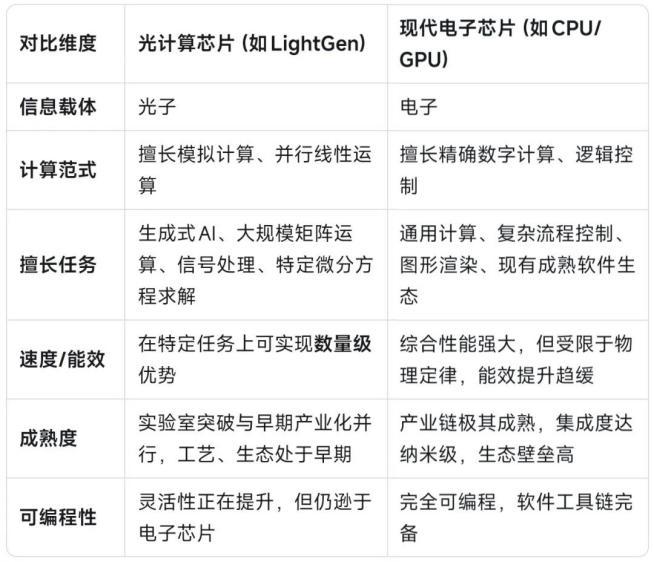
At present, the industry has basically reached a consensus: the training stage relies on GPUs (due to complex logic and high precision requirements), and the optoelectronic hybrid solution can be adopted in the inference stage. In this sense, the first pot of gold in the commercialization of optical computing chips is mainly tapped from the AI inference end. For example, in the field of artificial intelligence with larger computing capacity and higher rate requirements, as well as primary artificial intelligence tasks such as image recognition and speech recognition. In addition, meteorological monitoring, financial investment and other fields are also potential application targets.
Multiple Technical Routes Are Developing Rapidly, Which One Is Closest to Mass Production?
At present, the domestic optical computing track is flourishing, different enterprises are betting on different technical routes, and there is a clear gap in their implementation progress, but most of them focus on optoelectronic hybrid computing rather than all-optical computing.
Optoelectronic hybrid computing uses electronic circuits to take charge of control, storage and nonlinear operations, and optical devices only undertake linear acceleration tasks such as matrix multiplication and addition. Signals need to undergo electro-optical and optoelectronic conversion repeatedly at the chip boundary or between computing layers. This solution can effectively utilize the mature CMOS ecosystem, and is the mainstream solution that can be commercialized at present.
In the practice of industrialization, companies taking the optoelectronic hybrid route have achieved remarkable breakthroughs. Lightelligence has chosen the silicon-based MZI coherent optoelectronic hybrid computing route. The company launched PACE, the second-generation high-performance photonic computing processor, in December 2021, which pioneered the integration of optical chips and electronic chips, and first proposed the "new paradigm of optoelectronic hybrid computing power". From 2024 to 2025, the shipment volume of its optical computing chips ranked first in the world for two consecutive years. It is reported that Lightelligence has reached strategic cooperation with SenseTime, StepStar, Shenwan Hongyuan, Zhongke Tiansuan, and OriSpace, covering multiple AI application scenarios, aiming at full-link collaboration from underlying technology to upper-layer solutions.
The products of the American company Lightmatter are divided into three parts: photonic computing platform (Envise), chip interconnection product (Passage) and adaptive software (Idiom). Envise is the world's first photonic computing platform, each Envise processor has 256 RISC cores, provides 400Gbps inter-chip interconnection bandwidth, and supports PCI-E 4.0 standard interface, with good compatibility. The principle of the Envise processor is that light passes through the waveguide for computing, and each additional light source of a different color can correspondingly increase the computing speed. For example, if a red laser source can perform 1 million calculations per second, adding another laser source of a different color can double the speed to 2 million, and so on; and adding a light source hardly requires hardware modification.
It is worth noting that the Envise platform is not a pure photonic processor, but a hybrid optoelectronic heterogeneous system that combines mature CMOS technology and advanced silicon photonic integration technology, aiming to balance flexibility, programmability and ultimate performance.
The aforementioned Optical Core Technology currently has a photonic in-memory computing solution with leading matrix scale in public information. Different from the traditional MZI architecture, photonic in-memory computing integrates weight storage and optical computing units, which theoretically alleviates the "memory wall", reduces the power consumption overhead caused by repeated weight refresh, and has energy efficiency potential in continuous inference scenarios.
Different from the on-chip integrated silicon optical route, MemryX focuses on free-space optical computing, relying on spatial light modulators to achieve highly parallel optical operations. This technical route may be more suitable for scenarios such as end-side, vehicle-mounted, and industrial perception where the constraints on chip integration size are relatively loose and ultra-low static power consumption is pursued, without requiring highly complex heterogeneous integration of silicon optical wafers.
In terms of university scientific research achievements, as early as 2024, the Tsinghua team pioneered the distributed breadth intelligent optical computing architecture, and developed Taichi, the world's first large-scale interference and diffraction heterogeneous integrated chip, achieving 160 TOPS/W general intelligent computing. In June 2025, the team from the Shanghai Institute of Optics and Fine Mechanics, Chinese Academy of Sciences, innovatively solved the problem of "high-density information parallel processing on optical chips", integrating self-developed multi-wavelength light source chips, large-bandwidth optical interaction chips, reconfigurable optical computing chips, high-precision optical matrix driver chips and parallel optoelectronic hybrid computing algorithms, and successfully developed an ultra-high parallel optical computing integrated chip — "Meteor No.1", realizing an optical computing prototype verification system with parallelism greater than 100.
All-optical computing pursues to keep the optical signal in the entire computing link, trying to get rid of the loss of photoelectric conversion, and directly realize linear operations and nonlinear transformation in the optical domain. However, restricted by problems such as the lack of high-performance integrable all-optical nonlinear devices and the difficulty in scaling up optical storage, it is currently only in the laboratory verification stage.
Last December, the team of the School of Integrated Circuits, Shanghai Jiao Tong University, made a major breakthrough in the field of next-generation computing chips, and realized LightGen, an all-optical computing chip that supports large-scale semantic media generation models for the first time. According to the introduction, LightGen can fully realize the closed loop of "input — understanding — semantic manipulation — generation", complete high-resolution (≥512×512) image semantic generation, 3D generation (NeRF), high-definition video generation and semantic regulation, and support multiple large-scale generative tasks such as denoising, local and global feature migration.
Although the optical computing track continues to produce results and gather a large number of players, it is currently only in the small-scale pilot commercial stage, far from reaching the large-scale mass production level, which is mainly restricted by four major shortcomings. First, the process yield is low and the production cost is high, so the overall cost performance is not as good as mature GPUs. Second, the repeated conversion between electricity and light brings additional power consumption, which offsets the energy efficiency advantages of photonic computing. Third, the software ecosystem is fragmented, with high adaptation difficulty and high implementation cost. Fourth, the supporting core industrial chain is imperfect, and the production capacity and technology cannot support large-scale implementation.
Looking back at the development history of the computing power industry, every breakthrough in the computing power revolution is an iterative upgrade of the underlying physical carrier. From vacuum tubes to transistors, from single-core electronic chips to multi-core GPUs, now photons are opening a brand new chapter for next-generation computing power.
This article is from the WeChat official account "Semiconductor Industry Insight" (ID: ICViews), author: Feng Ning, published with authorization from 36Kr.