Running AI in glass: Research achievements of Huazhong University of Science and Technology and Shanghai Jiao Tong University published in a Nature sub - journal
Light is entering the AI computing power system. This time, it's not just used for data transmission but directly participates in the calculation.
The teams from Huazhong University of Science and Technology and Shanghai Jiao Tong University recently published their results in Nature Communications. They wrote a programmable photonic neural network inside the glass to construct a three-dimensional optical computing core.

This chip realizes direct on-chip optical processing of two-dimensional images -
The classification accuracy of MNIST handwritten digits reaches 93%, the fidelity of on-chip optical pattern generation is 94%, and the theoretical computational throughput reaches 6554 TOPS.
Its key architectural path is:
Two-dimensional space input → Three-dimensional light field mixing → Programmable phase regulation → On-chip neural network inference.
This is not only about making the optical matrix larger but also answering a core question - how to make the optical computing core larger, programmable, and capable of carrying real data.
Writing the photonic neural network into the three-dimensional space of glass
In the past few years, as the scale of AI clusters has continued to expand, the industry has mainly talked about optical interconnection when referring to light: using light to connect chips, boards, cabinets, and data centers to enable data transmission with higher bandwidth and lower power consumption.
This direction has become a very clear technological trend in AI hardware.
However, the value of light is not limited to "transmitting data".
Light can be multiplexed, coupled, interfered, and mixed during propagation. In many linear calculations, these physical processes themselves can become computational processes.
For the matrix calculations that are abundant in AI inference, light can not only be the medium connecting computing units but also potentially become part of the computing core.
The real difficulty is: what kind of optical computing core can amplify this advantage?
An optical computing system requires lasers, modulators, detectors, electronic controls, and packaging. If the scale is too small, it's difficult to spread these peripheral costs. If the structure is still limited to a two-dimensional plane, input, interconnection, waveguide crossing, and channel expansion will limit the chip scale.
In other words, for optical computing to truly move towards AI inference hardware, it's not enough to just prove that "light can calculate". It also needs to answer the questions of "how to make the optical computing core larger, how to make it programmable, and how to carry real data".
In 2023, Peter McMahon published a review in the Nature journal.

The article systematically sorted out various physical properties of light that can be used for calculation and pointed out that the advantage of optical computing doesn't simply come from "high light speed" but relies on the architectural design to simultaneously utilize multiple optical degrees of freedom.
This review led to a more specific question: which advantages of light are actually utilized by existing optical computing chips? And which degrees of freedom have not been truly unlocked?
This is the starting point of this work.
Based on this idea, the teams of Zhang Xinliang and Dong Jianji from Huazhong University of Science and Technology, in collaboration with the teams of Tang Hao and Xu Xiaoyun from Shanghai Jiao Tong University, wrote a programmable photonic neural network inside the glass to construct a three-dimensional optical computing core.
The relevant work was published in Nature Communications under the title "Programmable Three-dimensional Photonic Neural Network Chip".
This chip realizes direct on-chip optical processing of two-dimensional images: the classification accuracy of MNIST handwritten digits reaches 93%, the fidelity of on-chip optical pattern generation reaches 94%, and the theoretical computational throughput reaches 6554 TOPS.
The core of this work is not to make an optical matrix a bit larger but to verify a new architectural chain:
Two-dimensional space input → Three-dimensional light field mixing → Programmable phase regulation → On-chip neural network inference.
Where are the existing solutions stuck?
Photonic neural networks have been studied for more than thirty years.
In recent years, a large number of excellent works have emerged on planar platforms such as silicon photonics, thin-film lithium niobate, and silicon nitride. The academic and industrial circles have long reached a consensus that "light can perform matrix operations".
However, if optical computing is to truly move towards large-scale AI inference, it can't just stay in a small optical unit.
It must answer a more systematic question: how does data enter the chip? How are the channels expanded? How is the interconnection organized? How can the multi-dimensional degrees of freedom of light be transformed into a trainable, manufacturable, and scalable computing architecture?
The planar 2D structure encounters three very direct problems when expanding in scale.
Problem 1: Limitation of input dimensions
Data in the real world - images, video frames, sensor arrays - naturally have a two-dimensional or even higher-dimensional spatial structure. However, the input interfaces of many planar photonic chips are essentially still a set of limited on-chip channels.
To send a two-dimensional image into the chip, the data often needs to be unfolded, multiplexed, or serialized first and then enter the computing core.
This is a bit like rolling a picture into a line and then stuffing it into a pipe. The problem is not just that the input speed slows down. More importantly, the spatial neighborhood relationship and parallel structure that the data originally had are rearranged before entering the chip.
Light could directly utilize spatial channels to process information in parallel, but the planar input method compresses this advantage first.
Problem 2: Limitation of on-chip interconnection
After the data enters the chip, the optical signal still needs to propagate, couple, and mix between different computing units.
For small-scale devices, this is not difficult. However, when the number of channels increases, the waveguide arrangement on the two-dimensional plane will quickly become crowded.
In a planar chip, many connection relationships must detour or cross in the same layer. Detouring increases the path length and loss, and crossing brings crosstalk and additional insertion loss. The larger the matrix scale and the more complex the interconnection relationship, the more difficult it is to avoid these problems.
In other words, the planar structure is not incapable of optical computing, but when the connection relationship becomes dense, the two-dimensional space itself begins to become a constraint.
Problem 3: Limitation of scale expansion
The place where optical computing can truly play its advantages is large-scale parallel linear computing.
However, to further increase the scale, it's not enough to just add computing units. Input and output channels, control units, readout ports, and packaging interfaces also need to be increased simultaneously.
On a two-dimensional plane, these resources will compete for the same chip area.
Input and output occupy the boundaries, modulators and electrodes occupy the surface, waveguides occupy the routing space, and detection and readout also require interfaces. As the scale increases, the limitation no longer comes from a single device but from the congestion of the entire planar system.
Therefore, the problem with the planar structure is not that a certain link is "not good enough" but that input, interconnection, control, and packaging are all compressed into the same two-dimensional space. The larger the scale, the more obvious this geometric constraint becomes.
Behind these three problems actually points to the same fact:
Many photonic chips still organize light in a two-dimensional plane, while light can originally propagate, couple, and reconstruct in three-dimensional space.
There is also a deeper question here: why is three dimensions more natural for light than for electrons?
Electronic computing is also moving towards three dimensions, such as HBM, chiplet, TSV, and advanced packaging. However, the three-dimensional expansion of electrons is more about alleviating the distance problem between computing, storage, and interconnection.
Even in three dimensions, electrical interconnection still has to face resistance, capacitance, charging and discharging, thermal management, and synchronization complexity. High-density stacking can shorten some paths but won't eliminate these basic costs.
Light faces a different set of constraints. It's not without engineering challenges, but in a transparent medium, optical signals can organize information through three-dimensional spatial routing, mode coupling, and multi-channel parallelism without relying on large-scale wire charging and discharging like electrical interconnection.
This is the difference between three-dimensional optical computing and two-dimensional planar photonic chips, as well as traditional electrical interconnection architectures.
However, three-dimensional optical systems have also had their own problems for a long time: free-space optics is bulky, difficult to align, and sensitive to the environment, making it difficult to become a real chip-level system.
The core of this work is exactly here:
On the premise of maintaining chip-level integration, truly introduce three-dimensional spatial degrees of freedom into photonic computing.
These two things were previously considered difficult to achieve simultaneously.
Why glass, and why three dimensions?
Different from the industry's main use of glass for electrical interconnection in advanced packaging, this research work turns the glass itself into the space where calculation occurs -
The process of light propagating, coupling, and redistributing inside the glass directly undertakes the linear calculation function.
This idea is in line with the system logic behind directions such as CPO and optoelectronic integration: the boundary of the system functions undertaken by packaging is expanding, and this work provides an early prototype verification of glass extending its computing ability from an interconnection platform.
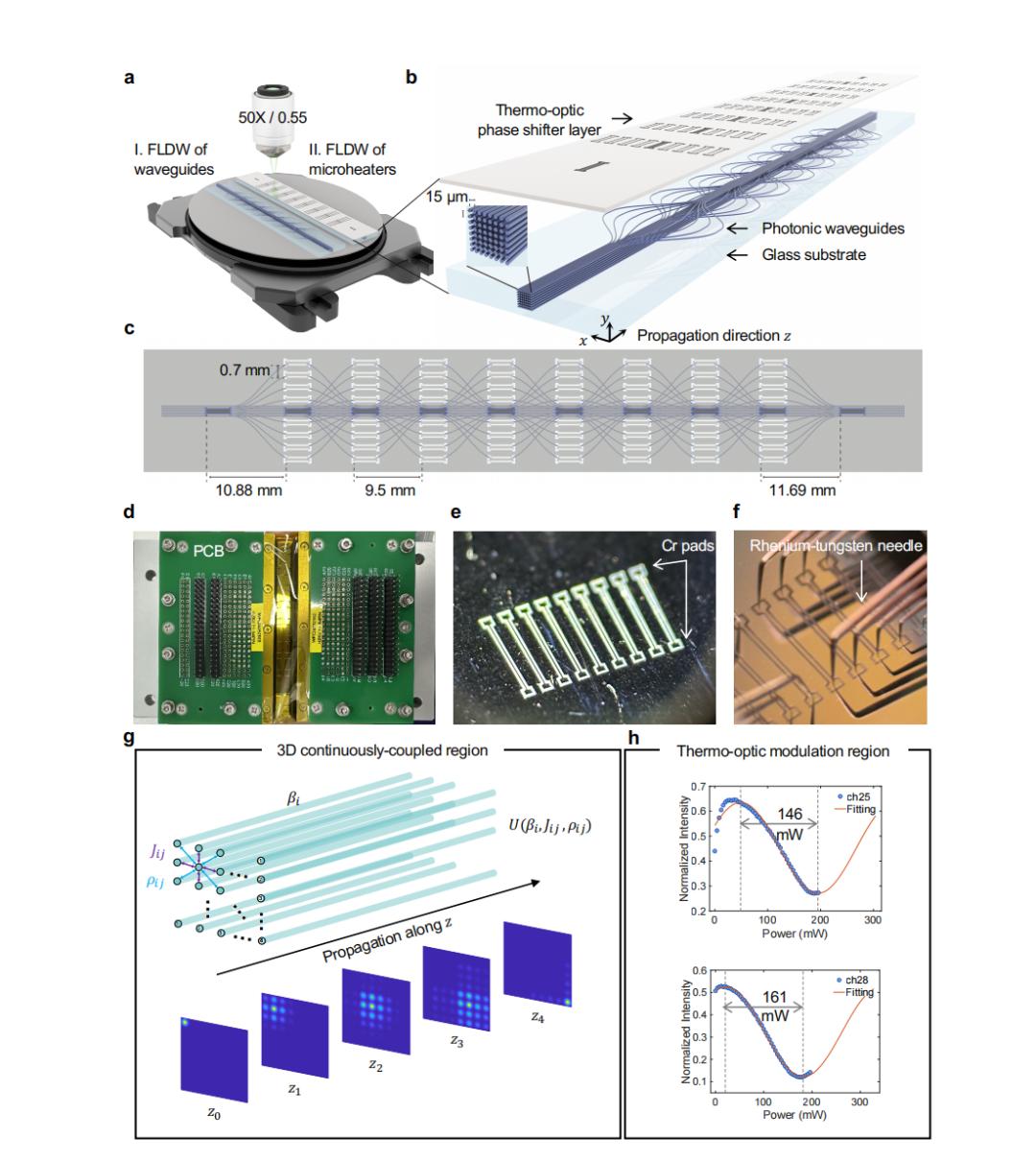
Femtosecond laser direct writing technology can focus an ultrashort pulse laser inside the transparent glass and locally change the refractive index near the focal point, thereby writing optical waveguides inside the material, just like directly carving a three-dimensional orbit of light inside the glass.
A traditional planar photonic chip draws an optical path on a piece of paper; this chip turns this piece of paper into a transparent volume.
Light can no longer only detour along the surface but can propagate, couple, and reconstruct between different depths. Therefore, the significance of this work is not just a change in material but a change in the geometric organization method of the computing core.
What did the research team specifically do?
The core architecture of the chip is composed of an alternating cascade of a three-dimensional photonic lantern waveguide array and a programmable phase shifter array, including a total of 8 cascade levels, realizing a three-dimensional optical network with an input-output scale of an 8×8 two-dimensional array.
There are two key modules here: the three-dimensional photonic lantern and the phase shifter array.
The function of the three-dimensional photonic lantern is to allow light to undergo multi-channel propagation, coupling, and redistribution in the volume space inside the glass.
It's not a simple power splitter that mechanically divides a beam of light into several equal parts;
More precisely, through continuous coupling between three-dimensional waveguides, it allows the input light field to mix between multiple spatial channels, thereby forming a multi-port linear optical transformation.
From the perspective of a neural network, this process is equivalent to completing the linear mixing in matrix operations through the propagation and coupling of light. The difference is that the connection relationship here is not mainly realized by in-plane waveguide routing but formed through the three-dimensional waveguide arrangement and coupling relationship inside the glass.
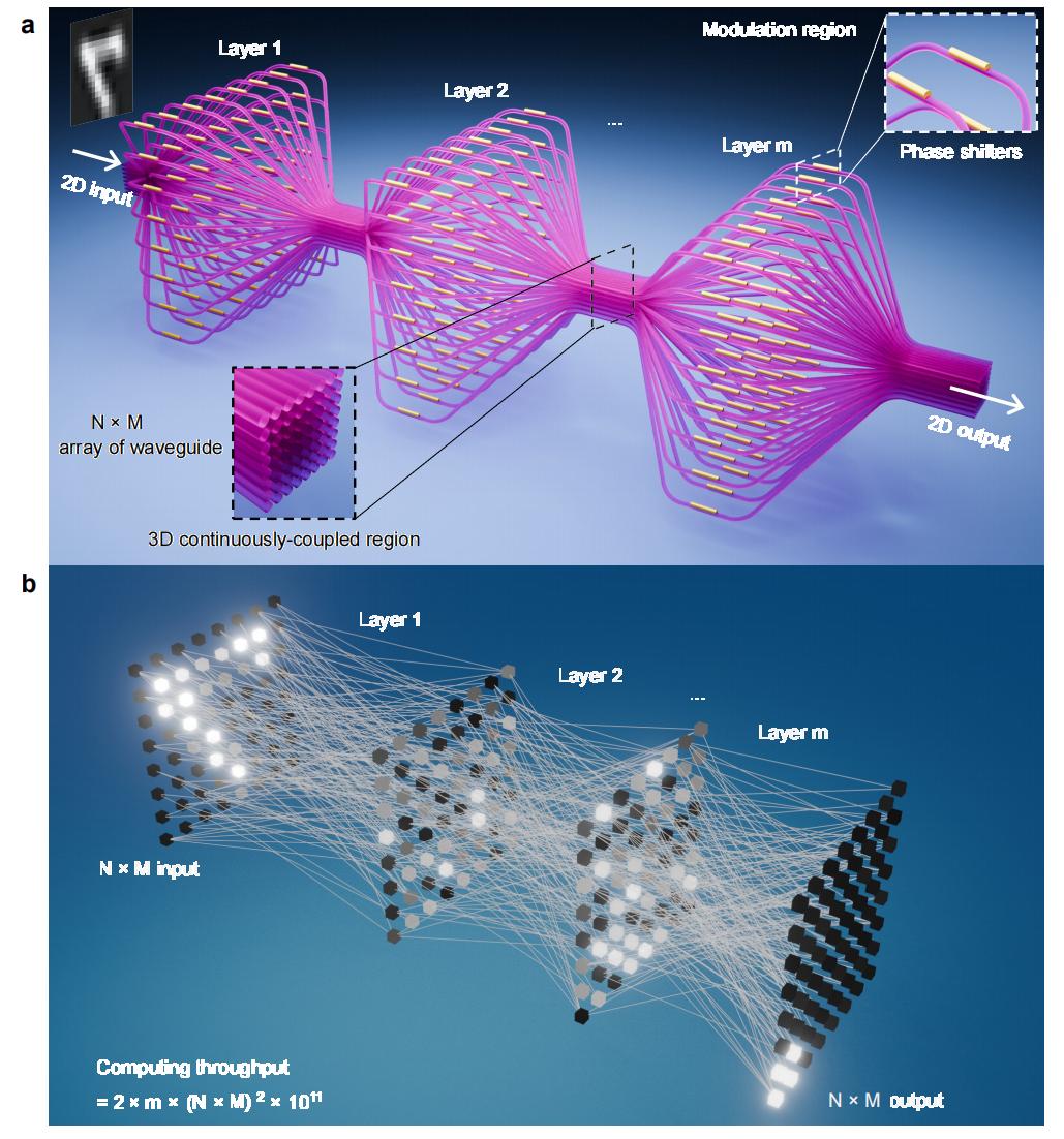
The phase shifter array is responsible for making this linear network programmable.
By adjusting the optical phase in different channels, the overall transmission response of the chip will change accordingly. That is to say, the same chip can adapt to different tasks through external training and electronic control adjustment without having to manufacture a new chip for each task.
In this architecture, the functions of these two modules are complementary: the three-dimensional photonic lantern provides complex spatial mixing, and the phase shifter array provides programmable control.
After alternating cascades, the three-dimensional mixing provides the "computing space", and the phase control provides the "training degrees of freedom". Together, they form a trainable three-dimensional photonic neural network.
Each layer of the cascade can be regarded as a "mixing - control" computational step: light first couples and redistributes in the three-dimensional lantern structure, then undergoes programmable adjustment through the phase shifter array, and then enters the next layer to continue propagating and mixing.
After multi-layer cascading, the chip can achieve more complex linear transformations.
To understand it in a more intuitive way: this prototype chip doesn't let light pass through a single plane once but allows 64 parallel inputs to undergo multiple rounds of three-dimensional mixing and phase adjustment inside the glass. Each round will change the distribution of the light field in space, and finally, an optical response related to the task is formed at the output end.
More importantly, it can receive image information in the form of a two-dimensional array.
In the experiment, two-dimensional image information is encoded into the input light field and coupled into the input waveguide array. That is to say, the image information doesn't need to be sent into the chip point by point through a one-dimensional serial channel but can enter the three-dimensional optical network after being encoded as a two-dimensional spatial array.
For data with a natural two-dimensional structure such as images, sensor arrays, and spatial light fields, this is very crucial.
This is also the difference between this work and many planar photonic neural networks: it not only uses a three-dimensional structure inside the chip but also tries to retain the spatial parallelism of two-dimensional data in the input method.
In summary, the architectural logic of this chip can be summarized as: retaining the two-dimensional spatial structure at the input end, invoking three-dimensional propagation and coupling inside the chip, providing trainable degrees of freedom through the phase shifter, and completing on-chip optical inference at the output end.
This is the specific meaning of "writing the photonic neural network into the three-dimensional space of glass".
Is the architecture really effective?
Whether this architecture is really effective was verified through multiple experiments and analyses in the paper.
In the MNIST handwritten digit classification task, the chip achieved a classification accuracy of 93%.
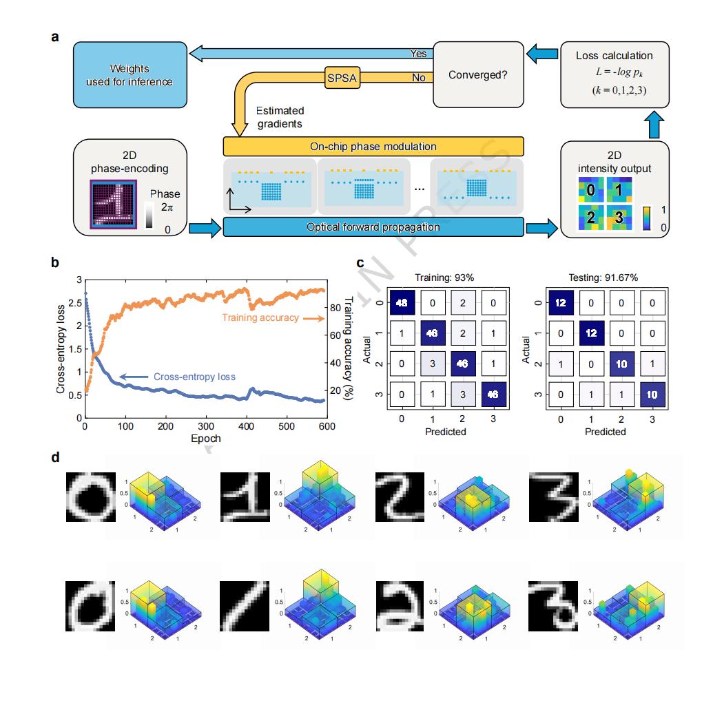
The focus of this result is not to directly compete with the software accuracy of mature electronic neural networks but to show that two-dimensional images can be encoded into the input array and complete a complete closed-loop from light field propagation, programmable control to classification readout in the three-dimensional photonic network.
The research team also demonstrated on-chip optical pattern generation, and the similarity between the output light field and the target pattern reached 94%.