The world model is here, and the old autonomous driving chips are starting to become ineffective.
In the past few years, there has been an increasingly obvious change in the automotive industry: Automobile manufacturers have started to produce chips on their own.
Tesla's FSD has been iterated to the fifth generation; NIO has launched the Shenji NX9031; XPeng has self - developed the AI Turing chip; Li Auto has created the Mach M100; BYD, Geely, and Momenta have also been frequently mentioned.
On the surface, this is a movement of "de - NVIDIA".
But if you only see this level, it's too superficial.
The real problem is: the autonomous driving model itself has started to change.
From CNN, to Transformer, and then to DiT and world models, the model paradigms are switching, and the chip logic of the old era may not be able to support the next - generation autonomous driving.
This is the real reason why automobile manufacturers are remaking chips.
01
It's not about saving money, but seizing control
Whether to self - develop or outsource is, on the surface, a business decision, but at its core, it's a judgment on the technical route.
Whether to self - develop or outsource depends on the car factory's judgment of the autonomous driving route. The chip R & D cycle is relatively long.
From the complete definition of the design goal to the mass - production of the chip in the vehicle, it takes 2 - 4 years. It takes even longer for overseas manufacturers, perhaps 3 - 5 years.
This means that when chip manufacturers start their work today, they are actually betting on the technological trend 5 - 8 years later.
If the prediction is wrong, either the chip's lifecycle will be significantly shortened, or no one will use it at all.
Making automotive digital chips is really a high - stakes gamble.
When automobile manufacturers self - develop chips, in a sense, they are saying: I know better than the suppliers what models I will run five years later.
The one - time engineering cost and external procurement of IP for 5 - nanometer or even 3 - nanometer chips can be as high as hundreds of millions of RMB. The one - time engineering cost plus IP licensing often amounts to hundreds of millions of RMB.
If the shipment volume is not enough, there will definitely be a loss on the books. But this money can be included in the overall R & D cost, and it can also boost the market value and strengthen the technology brand.
In the end, the business logic makes sense.
In terms of technical threshold, with the maturity of the IP ecosystem, the improvement of the EDA toolchain, and the emergence of intermediaries like Socionext that specialize in serving car factories for customized chips, the engineering difficulty is rapidly decreasing.
The really difficult part has shifted to the software stack, compiler, and long - term model adaptation, which are precisely the parts that chip suppliers find it most difficult to customize for you.
02
The model has changed,
and the chip logic has to change too
First, figure out what models are currently being run in autonomous driving.
There are currently three autonomous driving routes.
One is the segmented end - to - end route, which is the choice of most manufacturers. A typical representative is Uni - AD, and the total number of parameters generally does not exceed 500 million.
The second is the VLA route, which is a vision - language - action model, combined with a diffusion action expert or MLP, and fuses the world model to improve inference efficiency. VLA usually has a MoE architecture, and the number of parameters is generally between 2 and 7 billion.
The third is the world model plus diffusion action expert route. There are currently no mass - production cases in vehicles, and the waiting time may be longer than expected.
The chip requirements of these three routes are completely different.
Moreover, no manufacturer bets on only one route.
All three routes are being explored, and no one dares to fall behind.
There is a widely - spread misunderstanding here: as long as the TOPS value is large enough, it can handle all models.
This was indeed the case in the CNN era. When the computing power was increased, the performance would improve. But today is a hybrid era of CNN + Transformer, and tomorrow may be the era of Transformer + DiT.
A 5000 - TOPS chip running the DiT architecture may well be outperformed by a 300 - TOPS competitor.
What determines the outcome are the memory bandwidth, orchestration ability, tightly - coupled hierarchical memory, SFU, and programmable vector computing power. Each of these is more important than the TOPS number.
The worship of TOPS is becoming ineffective.
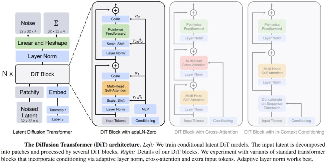
The core of the world model is the DiT architecture
03
New troubles brought by the world model
The third route was truly formed last year. Its core architecture is called DiT.
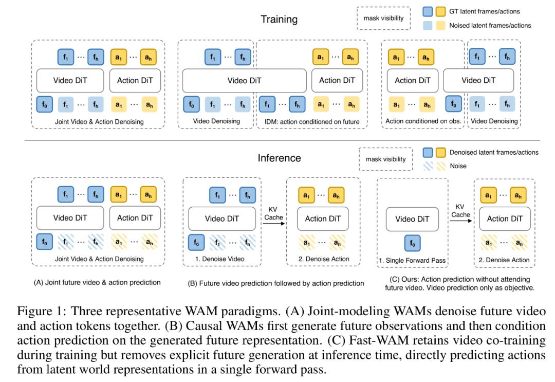
The typical architecture of the world model. The above image is from the paper Fast - WAM: Do World Action Models Need Test - time Future Imagination?
Why is the world model special?
Because DiT has a natural affinity for temporal information. It is not just a "better image generator", but an architecture tailored for videos, animations, and even autonomous driving and embodied intelligence.
Whether it's joint modeling, imagining first and then executing, or "modeling during training and directly outputting actions during inference", DiT is the core of any world model paradigm.
The problem is: There are no chips specifically designed for DiT inference on the market.
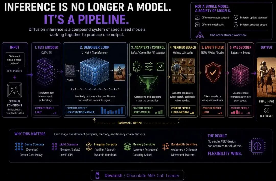
The inference process of the diffusion model
The inference process of the diffusion model is extremely complex.
Traditional high - computing - power chips can only handle dense tensor matrix multiplication, that is, the calculations inside the denoising loop.
The remaining irregular calculations, vector encoding, and memory - sensitive activations either rely on scalar CPUs or vector algorithms, which pose a severe test to chip design.
If an automobile manufacturer is determined to follow the world model route and doesn't want to wait for a suitable chip to appear on the market, there is probably only one way: self - development.
04
Memory bandwidth is the real bottleneck
There is a detail worth discussing separately.
Regardless of the technical route, the wider the memory bandwidth, the better.
The VLM (Vision - Language Model) is the most typical example. The decoding stage is the main time - consuming part of the VLM, and the decoding speed is completely determined by the memory bandwidth.
In other words, the overall performance of the VLM is essentially the performance of the memory bandwidth.
This is why Tesla's AI4/AI5 spare no expense to widen the memory bandwidth. They know very well where the real bottleneck lies.
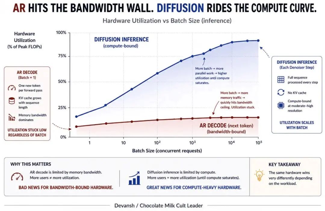
The decoding stage of the autoregressive (AR) architecture is memory - bound. No matter how high the computing power is, it cannot be accelerated. The system performance completely depends on the memory bandwidth and scheduling delay. In this stage, some small models may even run faster on the CPU than on the GPU.
The diffusion model faces another dilemma: it highly depends on the Batch size (the number of concurrent batch processing). The larger the Batch, the higher the utilization rate of the matrix multiplication unit. But when the Batch is large, the irregular operations and scheduling consumption outside the denoising loop will skyrocket, and the overall delay will increase significantly.
In the delay - sensitive autonomous driving scenario, the Batch is usually set to 1 - 4, rarely exceeding 8. As a result, although the GPU has amazing computing power on paper, it actually idles a lot.
05
Large cores, medium cores, and small cores:
Three computing philosophies
The core of the autonomous driving chip is the AI accelerator. And the dispute over the route of the AI accelerator is essentially a collision of three computing philosophies.
According to the M×N×K dimensions of a single matrix multiplication ALU, there are currently three schools: large cores, medium cores, and small cores.
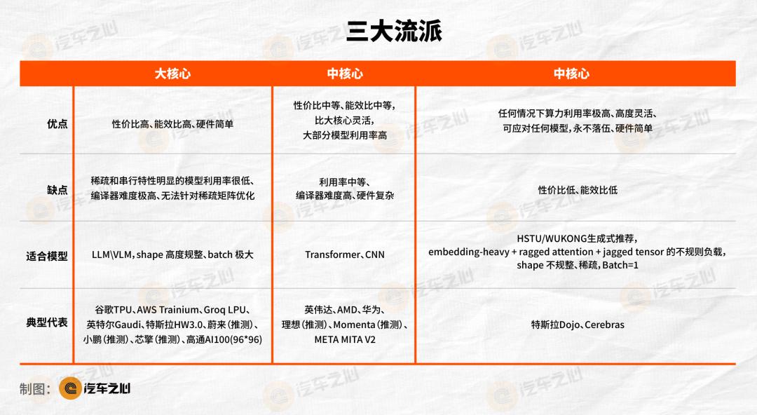
(1) Large cores: Extreme efficiency - oriented
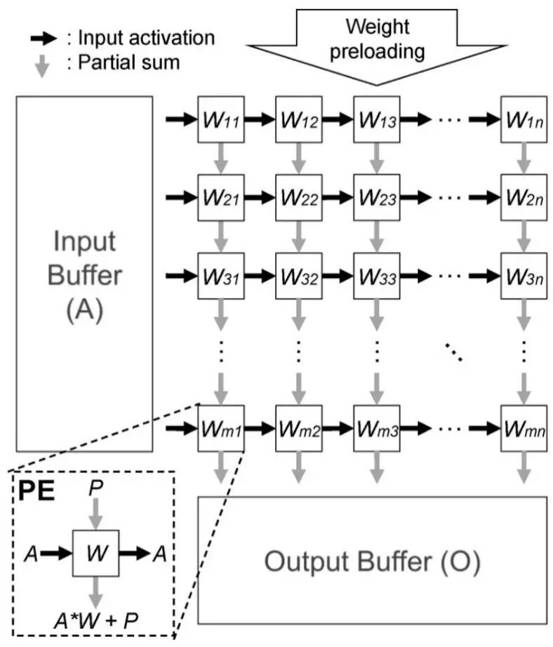
The typical large - core architecture is the systolic array.
Google's TPU v5/v6 has a 256×256 array, and each core has 65,536 MAC arrays. The data only flows in once and is transmitted forward along the pulse. The SRAM reading pressure is much lower than that of the small - core solution. When running models like LLM/VLM with highly regular shapes and extremely large batches, it leads in terms of energy efficiency and cost - effectiveness.
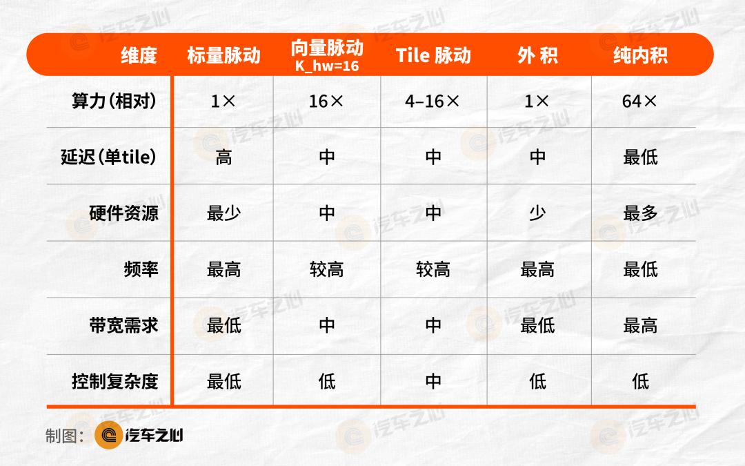
Typical representatives: Google TPU, AWS Trainium, Groq LPU, Intel Gaudi, Tesla HW3.0, NIO Shenji, XPeng Turing, Xinqing, Qualcomm AI100.
The frequency of each array of TPU v5 is 1.5GHz, and the single - core computing power is about 197 TOPS; v6 is upgraded to Tile systolic, and the single - core computing power reaches 918 TOPS at the same frequency. Each instruction drives 65,536 MAC operations, leading overwhelmingly in dense matrix multiplication.
The cost is also obvious. The large - core is more like a super - large assembly line. When the data shape is regular enough, the efficiency is extremely high. Once the model structure becomes sparse, dynamic, or irregular, the assembly line starts to idle.
The disadvantages of large cores are also obvious. First, they are highly sensitive to the data flow shape, or rather, the matrix shape. The 256×256 array requires that M, N, and K must all be integer multiples of 256. If not, tile splitting, padding, layout transformation, double buffering, and collective operations are required.
The 256×256 array requires that M/N/K must all be integer multiples of 256. A slight deviation requires a large number of pre - processing steps.
If the compiler is poorly designed, it is not uncommon for the computing utilization rate to be as low as 10% or even 1%. Even if well - designed, it is difficult to exceed 40%. Running a model with tens of billions of parameters may take the same time as running a model with tens of millions of parameters. The software team is more than ten times the size of the hardware team. This path has extremely high personnel - training costs, and losses are almost inevitable.
Another major drawback:
It is completely ineffective for unstructured sparsity. Autonomous driving vision models are typical sparse models, while large cores are typical dense engines.
Google's TPU v6e has added a sparse tensor core for this purpose, but this will inevitably increase software complexity and scheduling time.
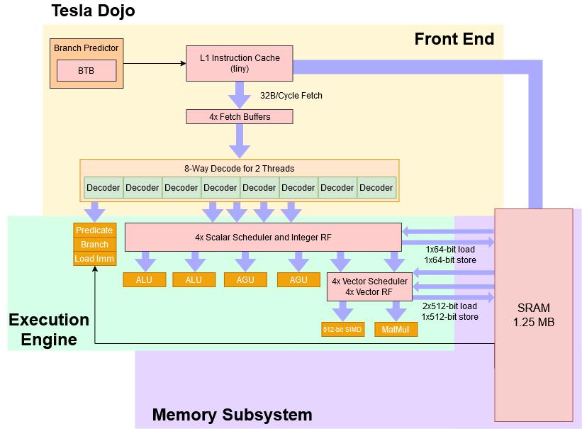
(2) Small cores: Extreme flexibility - oriented
Small cores are actually multi - core CPUs.
The extreme representative of small cores is Tesla's Dojo, which is essentially a collection of 384 - core CPUs, with each core having an independent branch, loop, PC, and local SRAM.
Its natural advantage is that it can easily handle data of any shape.
It can maintain a high utilization rate even when batch = 1. It is naturally suitable for decoding, MoE expert routing, and variable - length KV cache. It natively supports unstructured fine - grained sparsity.
A report from Cerebras shows that at a 75% sparsity level, it can achieve about 2.5 times the actual acceleration compared to the dense baseline, which is impossible to achieve with the large - core architecture.
The cost is also obvious. Each small core has the overhead of independent instruction fetching, decoding, register file, and control logic. With the same process and the same computing power, a pure small - core design requires 2 - 5 times more area than a systolic array, which means that for the same computing power, the cost is 2 - 5 times higher.
This figure is enough to deter most manufacturers. So there are very few manufacturers actually taking the small - core route.
(3) Medium cores: Balanced approach
NVIDIA has chosen the third path - neither extreme, nor a dead - end.
The GPU has a 16×16 matrix unit. The number of medium - core Tensor Cores on an H100 is more than that of large cores but far less than that of CUDA cores. The medium - core Tensor Cores are responsible for dense computing power, while the small CUDA